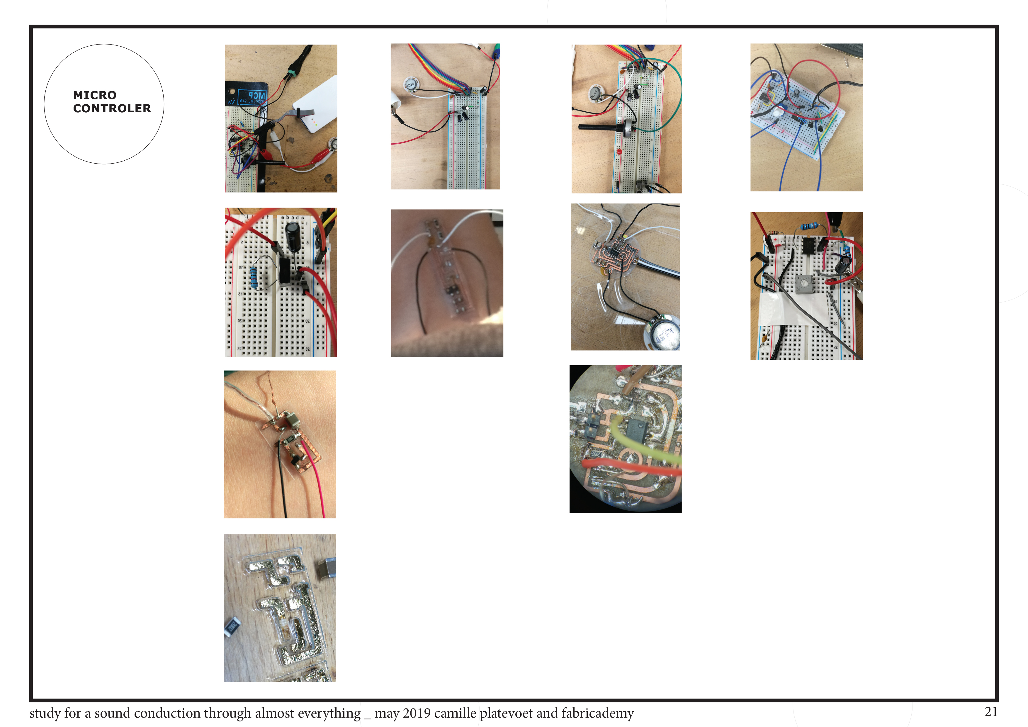
Process microcontroler#
| Circuits |
|---|
 |
 |
 |
| File PCB Square .zip | .png |
|---|---|
| Laser cut files LM 386 Trace PCB .zip | Laser cut files LM 386 Trace PCB .zip |
| File Fabric lasercut .zip | PCB .pdf |
|---|---|
| Laser cut files LM 386 circuit contour .zip | Laser cut files LM 386 circuit contour .zip |
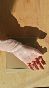
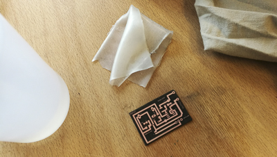
Circuit substract#
To put the circuit on the skin directly like a jewellery piece I search the good substract, and materiality. I would like to make a gold tattoo circuit, but It’s too complicated for me now, but you will see that I have tried a little. I’m close to find the solution !
| Make a classical circuit | Manage an own circuit process technic |
|---|---|
| Strong, Stable, non-visible, small | Flexible / Pliable / Soft / Curve / Paper, visible, stable, embodyable, wearable, doable… Be sure that my goal is to make a circuit in an way where the circuit is on Bio material and which is possible to put on the skin directly and follow the movements of the body |
Circuits video archives with differents shapes#
Circuit test list process of the differents base/substract#
| List of my circuits tests | Conclusion | see my documentation |
|---|---|---|
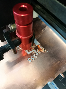
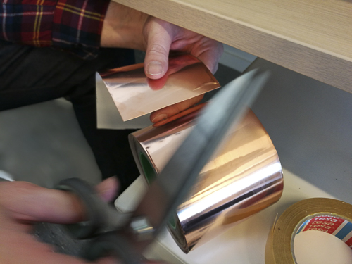
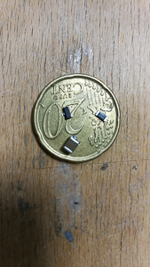
| copper shield | stable, need largest traces, the temperature to solder it is between 280 °C | my final project |
| copper tape | vynil cutter are broken | my final project |
| fr4 1.6mm | good for prototype or the scale of the furniture / machine farication 330 °C | final project |
| fr4 0,8mm | same | final project |
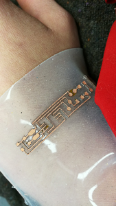
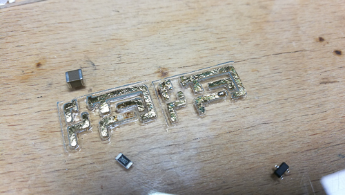
| gold 4carrat thread | it works, it’s beautiffull but it is not the space to do that, I haven’t the tools yet | off line |
| gold sheet 24 carrat | it’s working, but I need time to explore and my purchases with wire glue take time to fix the components like microcontroler on the traces I can solder on it with simple LED | skin electronic/wearable |
| copper sheet | same | final project |
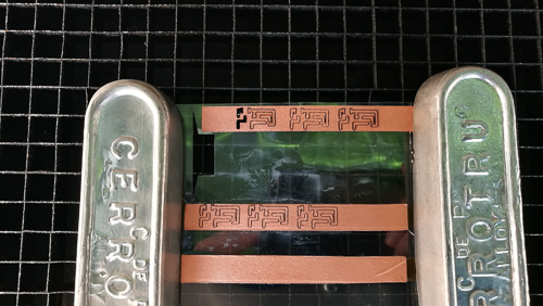
| biomaterial and copper shield | the temperature 250 °C is very difficult to control but it’s working ! | final project |
| added capton every time is possible | to insulated the heat | final project |
Silicone#
| Layer of silicone | layers of copper fabric Shield | On skin directly |
|---|---|---|
 |
 |
 |
Video silicone and copper shield layer#
| Test with vynil cutter | Tips for machine | Parameters | On vynil | Result | Result |
|---|---|---|---|---|---|
 |
 |
 |
 |
 |
 |
| Just a little part of the cutter is outside, to make the zero machine put the button outline, move the axis and put it again online. The copper tape is put on a layer of special material to move easly betweens the rolls. | Copper tape bobine | Parameters for copper tape | Parameters for vynils | Problem with the software, the machine doesn’t finish the final line. | copper |
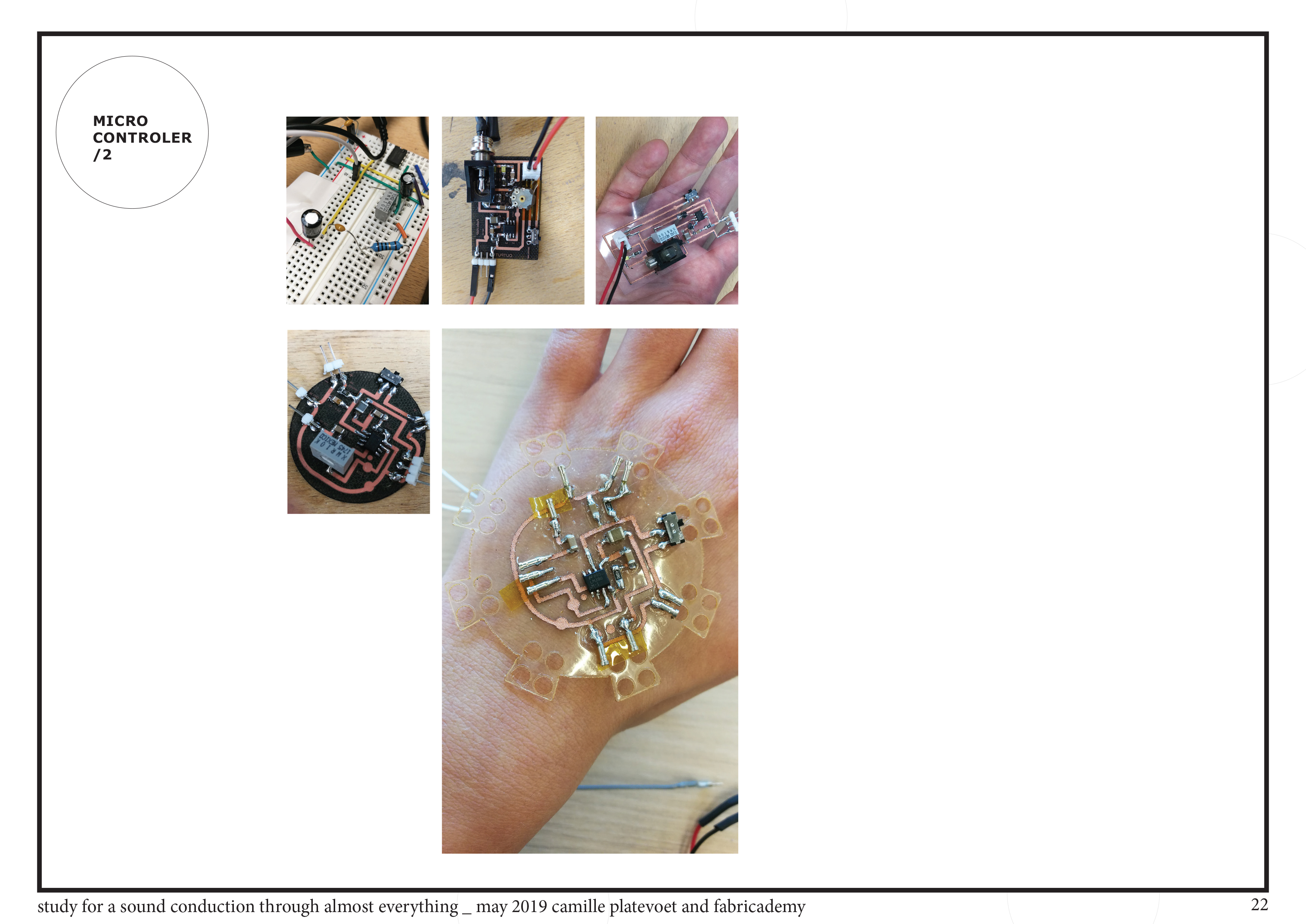
Multilayered Capton Copper Shield Silicone : Fab Material flexible circuit#
| flexible circuit | copper shield |
|---|---|
 |
 |
| Mutlti layer material | Capton | Copper fabric | Base with silicone or sheet transparent | Machine parametters |
|---|---|---|---|---|
 |
 |
 |
Epilog Fusion CO2 Vector 12/10/100 |
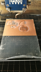
Test with gold sheet#
| Test with gold to see the skin electronic WK12 on cotton | Epilog LaserCut | Machine parameters | Interest |
|---|---|---|---|
 |
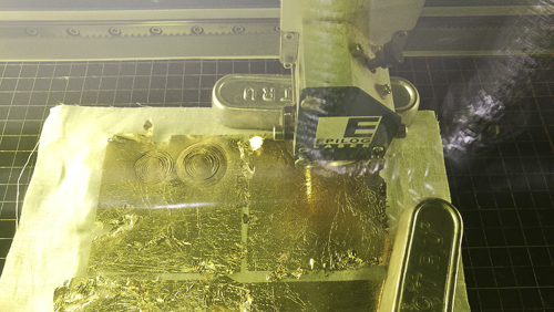 |
Epilog Fusion CO2 vector 15/10/100 | Gold is super stable, for the trials I use copper sheet. It’s stable for electronic and for skin : STAINLESS |
See below the result with component, also week 5 LED blink and week 12 for the process.
| Research |
|---|
| Flexible circuit mesure heart pulsasions |
| Gold circuit grid tattoo |
| Kobakant conductive fabric research |
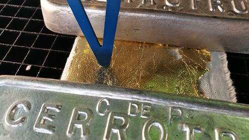
| Test on gold circuit *** | Conclusion |
|---|---|
 |
on cotton fabric I think it’s too thin, doesn’t resist to solder |
See the part Week 12 for the gold technic part.
Result from the tests#
| To compare | Details |
|---|---|
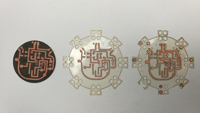 |
the pcb in FR4 0.8 mm is to confirm that the circuit in this smaller size is working. The circuit on the center is laser cuted separetly, the traces are applicated after the lasercuted process. The last one is with capton and the other with capton and lasercut on the bioplastic directly. |
Electronic : The steps in the research technic process#
The process to find the good electronic component was to find how I can do and for which functions. I’m interested about the sound to medicine application (like frequency), but also sound for universal way to communicate feelings, implications, culture.
1 Amplifier#
Process step :
Since the 15 th of January I’m In that process, to learn the movement from electrons, and the music they can do in their travels. It’s a little big part. But to design an object / a project, I like to “control” or “understand” what I’m doing, why I will do and then I can choose the way of the project growing.
| Number | Electronic | Protoboard | SMD size |
|---|---|---|---|
| 1 | With a mosfet TIP 120 | ok | the result was not working with a smd size. |
| 2 | With an Attiny 84 | ok | It’s a poetry with hertz and frequences it’s funy but my work can be just on a frequency research because I need to work with medical team to follow this project |
| 3 | With an Op Amp LM4861 | ok | It doesn’t work with a smaller size after 1 week of research |
| 4 | With a 555 | it’s a good frequency vibration (Jonah’s research and help) ok | not test |
| 5 | With a MCP6241 | problem with the amp signal value | not test |
| 6 | With a LM386 | ok | ok |
RULES FOR EAGLE AND PCB PROTOCOL MAKING !!!!#
I would share my favorite rules that I have learn myself during this crazy process :
- Protoboard then 12 06 it’s already a big step !
- check the size for the component in real and in eagle (eagle is malign !) 1206/1208/smd blablabla
- space for solder
- space for the iron solder !
- heat the trace and the component
- visibility of each component and solder
- make one large set up with space for traces and for components, then test
- make a smaller device as possible then test
- 2/ then reduce the size of the traces
- do not put a component on a trace directly but in a space close to the trace
- text size 0.6mm
- add the polarity on cap (more than 1uf)
- add test area for the Oscilloscope
- add test aera for the gnd and vcc test
- add led : it’s a good visual signal to know what’s happening with the electrons ! Many Many lights !
It’s useless to make the smaller pcb as possible for a new circuit on the first test. Respect the rules and the time of the work space and your brain time !
1 TIp 120#
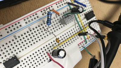
| Piezo and input | Proto board | Cap 1uF + TIP120 + R |
|---|---|---|
| Amplifying without an amp | basic mosfet circuit | detail for the basic mosfet amp on a protoboard |
 |
 |
 |
A TIP120 is a type of MOSFET, which is a kind of electronic switch. I wanted to see if a MOSFET could be used for aamplifying sound.
To be able to make this circuit as tiny as possible, I use Eagle PCB to make the schematic and Illustrator to convert the file for the laser engraving machine.
| Eagle Traces | Vectorisation using Illustrator | Exporting without compression |
|---|---|---|
 |
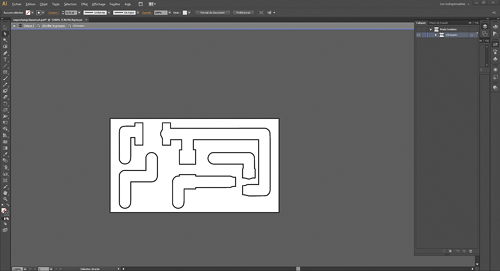 |
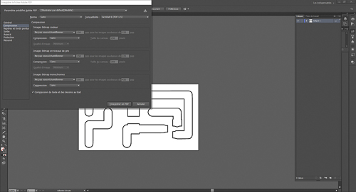 |
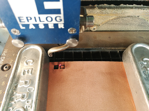
The Fablab Digiscope has a laser engraving machine which can work on metal. We start with a blank PCB board and then engrave away the copper to leave our cicuit at the end.
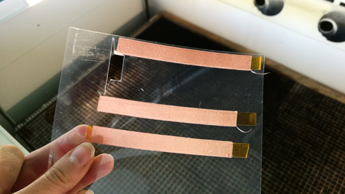
I was interested to explore engraving on flexible PCBs, instead of the standard epoxy boards. To work with this flexible fabric I adhered it to a thin sheet of arylic plastic.
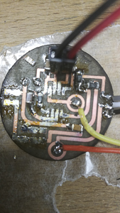
| Testing Copper Fabric on the Epilog Fusion | Cutting the circuit on multilayer material | Laser Cutting Result |
|---|---|---|
 |
 |
 |
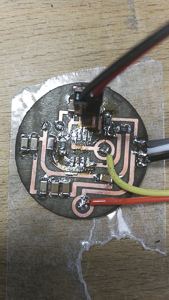
| Circuit | Component | Solder |
 |
 |
 |
Once I cut the copper fabric, I began trying to solder on components in the electronics lab.
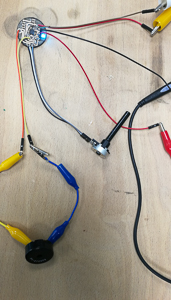
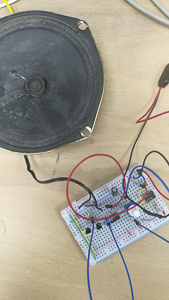
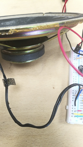
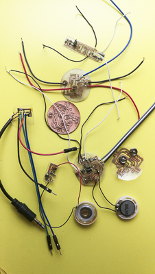
| Sound amp device components | Wearing on the skin | Entire device |
|---|---|---|
 |
 |
 |
| - | - | - |
| Tools | Cap 100uF + MOSFET + Resistor 20kOhm + Copper Fabric + Capton tape + Audio-In Jack + 8 Ohm Speaker |
I’m using 1206 SMD components that measure around 1cm x 2cm. This was a feature because it helped me imagine hiding this circuit in a piece of clothing.
Several questions arose in the making of this circuit. For instance:
Can we wear the circuit on the skin, to be able to control the volume better ?
I discovered that connections are the problem for a circuit like this. Where should wires connecting to the input, the speaker or the power be positioned?
2 Attiny 84#
- Download : ATMEL Studio
| ATtiny 84 Tutorial |
|---|
 |
I attended a tutrial which provided an introduction to microchip architecture.
We covered Hexidecimal notation, registers, how to flash code onto the chip, etc.
| ATtiny programmer with Atmel Studio | p. | p. | p. | p. |
|---|---|---|---|---|
 |
 |
 |
 |
 |
This is a helpful book to understand the useful steps to follow to communicate with AVR Microhips.
| Proto board | Zoom | Signal |
|---|---|---|
 |
 |
 |
This is a more advanced circuit than the previous one I attempted.
I use Attiny84, a potentiometer, resistors and capacitors, and a single MOSFET TIP120.
With the potentiometer I can change the frequency of the output signal. On the oscilloscope I could observe the output signal frequency in real time as I turned the potentiometer.
| Code with C | Second part of code | Parameter for board | Parameter for ATtiny84 and ISP Programer |
|---|---|---|---|
 |
 |
 |
 |
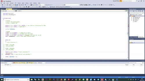
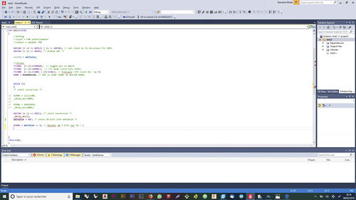
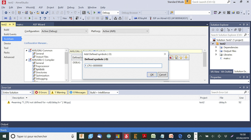
I’m using AVR Studio to program the Attiny84 in C code.
After uploading the code, I changed the fuses to set the clock speed.
 /*
 * Attiny84 analog read.c
 *
 * Created: 19/01/28 2:20:06 PM
 * Author : camille
 */

#include <avr/io.h>
#include <util/delay.h>


int main(void)
{
    //analog
    //input = PA0 potentiometer
    //output = speaker PB2

    ADCSRA |= (1 << ADPS2) | (1 << ADPS0); // set clock to 32 divisions for 8MHz
    ADCSRA |= (1 << ADEN); /* enable ADC */

    uint16_t adcValue;

    //chrono
    TCCR0A  |= (1<<COM0A0);  // toggle pin on match
    TCCR0A  |= (1<<WGM01);  // CTC mode (once hits OCRA)
    TCCR0B  |= (1<<CS02); // Prescale: CPU clock div. by 256
    DDRB = 0b00000100; // PB2 is OC0A (HOOK UP BUZZER HERE)

    while (1)
    {
    /* start conversion */

//  OCR0A = 11111100;
//  _delay_ms(1000);
//
//  OCR0A = 10101010;
//  _delay_ms(1000);

    ADCSRA |= (1 << ADSC); /* start conversion */
    _delay_ms(1);
    adcValue = ADC; /* store 10 bits into adcValue */

    OCR0A = adcValue >> 2; // decaler de 2 bits sur 16 / 2

}
return(0);
}
This code uses timers (in the chrono section) to create variable frequencies I could control by changing the bit value of a register.
Attiny84 Video#
Attiny84 Video showing oscilloscope reading sound frequency#
Attiny84 and a piece of GOLD !#
I have replaced a portion of wire in the electronic device with a piece of gold-plated wood, like a wire.
3 Op AMP LM4861#
Research from fabacademy student and tutorials which informed this experiment#
- Project : Fabacademy mrehan-Elshehawy
- Project : Nadya Amp
- Project from instructable : Bones conductor
| Op Amp | Data sheet | Power |
|---|---|---|
| LM4861 | Data Sheet | 3-5.5V |
Process :
- 1 gather the components in the circuit part list
- 2 etch the circuit and solder the components (heat 330°C)
- 3 test it to see if it works
- 4 Debug test all the routes with the multimeter in continuity testing mode (buzzer activated)
- 5 Debug test the ohm values of the resisor and the Farad values of the capacitors
- 6 Replace components like battery, sound, cables to see if they were defective…
- 7 Debug replace the microchip (black box)
- 8 Check the routes once again
- 9 tips, add LEDs to see where current is flowing
- 10 Oscilloscope is very usefull for visualizing !
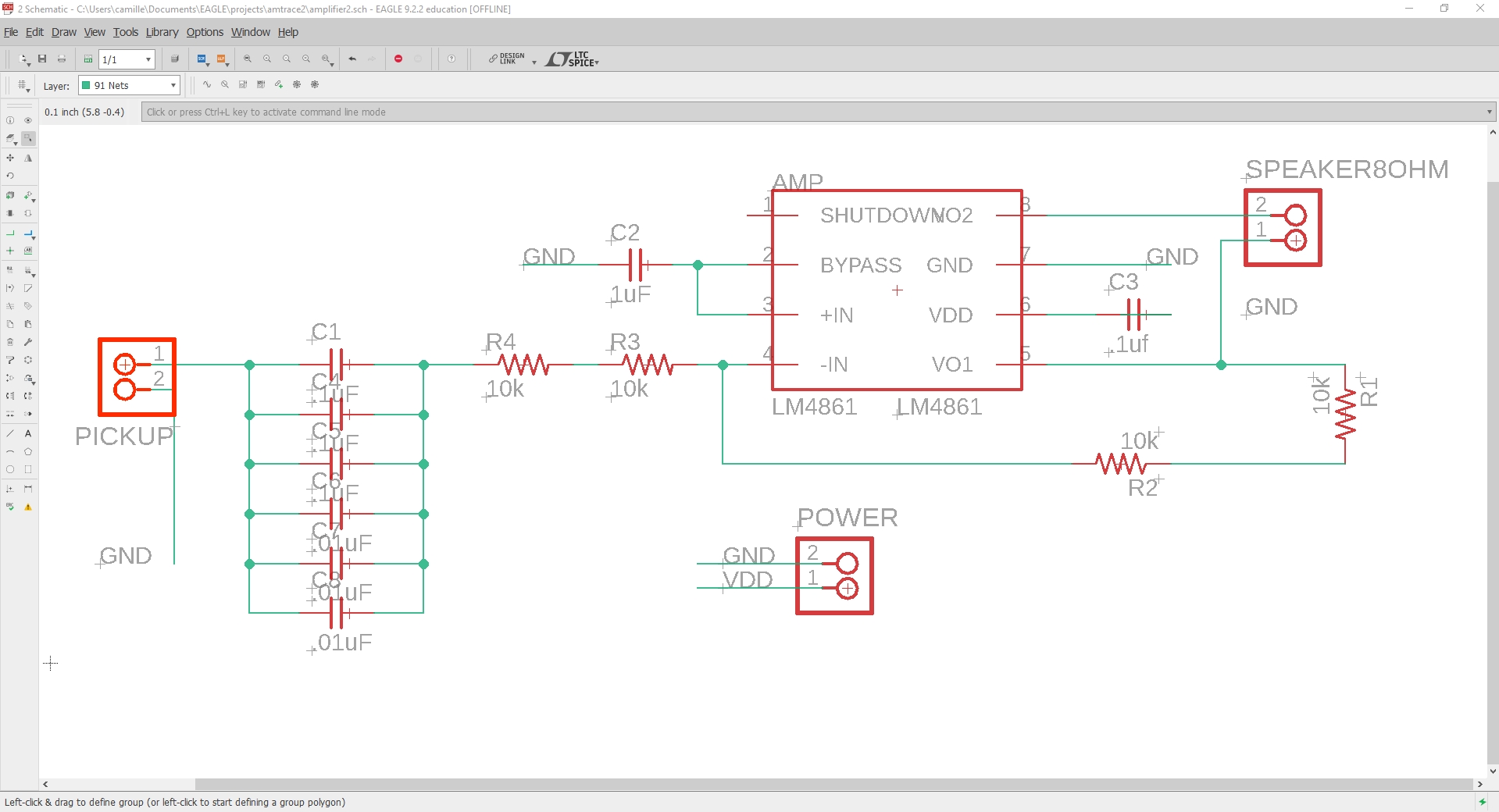
| Test 1 Eagle board schematic | Op amp LM 4861 thin board in Eagle |
|---|---|
 |
 |
I chose two tutorials to inspire my own circuit. I tried to make my first test as small as possible (I think this was a mistake, when making a circuit for the first time it shouldn’t be too compact).
| Protoboard | Detail | Add potentiometer and button |
|---|---|---|
 |
 |
 |
After cutting out the board, I decided I should restart qnd first prototype the circuit on a breadboard. I used a set of clips to plug in the opamp which was too small to fit into the breadboard.
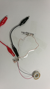
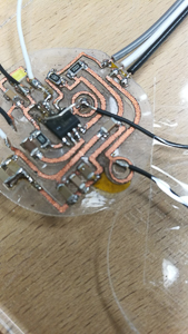
| Flexible circuit with copper shield |
|---|
 |
My first attempt at a compact size of the circuit. I got stange readings of the capacitors and resistors using the multimeter while debugging.
LM4861 + Signal 2V oscilloscope#
As you can see, the prototyped version of the circuit works well.
LM4861 + input jack plugged-in and an LED#
Second Test with a pcb board#
| Eagle final Circle Shape 40 mm | Schematic |
|---|---|
 |
 |
After the first PCB test, I decided to make a second attempt with the stanard epoxy PCB and a less compact circuit design.
| Pcb | OpAmp 1 pin soldered | Solder the 4 ext pins | Final | Test | Result |
|---|---|---|---|---|---|
 |
 |
 |
 |
 |
The led is ok, but it doesn’t amplify |
Making this board, I learned how to solder perfectly and, also, that the debug process takes time.
| Change the Op Amp | Change the Op Amp + the capacitors | Conclusion |
|---|---|---|
 |
 |
After we observed the signal and the values of the various components we switched each of the components out one by one. This experience was stressful as it was near the deadline for the end of the course. |
| Soft Multilayer material | Add connections | positioning the circuit near the ear | the various wires needed |
|---|---|---|---|
 |
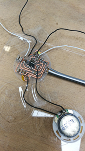 |
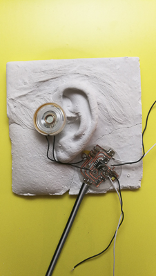 |
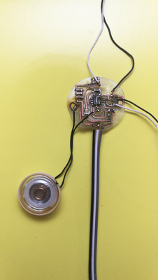 |
Debuging Process#
After the process of testing mutliple characteristics of the circuit in order to debug the problem, the only thing we found to be odd was our reading of the resistor values in the circuit which were different values that what we needed.
This device seems to work well on protoboard with normal sized (through hole) components, but in the 1206 size with the same components it doesn’t work for us.
The long debuging process told us that a resistor value we read from the circuit was not what we had hoped but after we had changed the value with an other, the circuit still did not work. The problem must have been elsewhere and we were not able to locate it at this time.
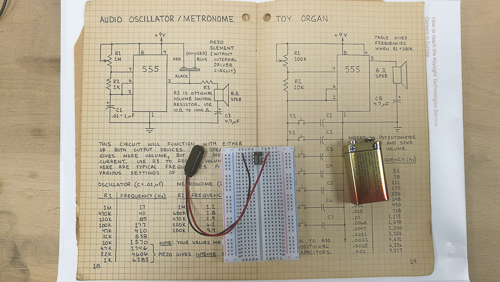
4 555#
| Forrest Mimm’s Engineering Book | Protoboard | 8ohm Speaker |
|---|---|---|
 |
 |
 |
We found a cool book which gave examples of clasic 555 timer circuits. I decided to make the Audio Oscillator circuit from the book.
Conclusion#
| Conclusion | Coments |
|---|---|
 |
I have tested different circuits, with different components and microcontrolers. I have had trouble making cicuits work with SMD size components. Our device in protoboard format works, so I have decided to make my test circuit from a laminate of copper fabric and kapton tape. I have learned that we need to be super carefull with the protocol. Try first with a protoboard, then PCB in epoxy in large size, then flex pcb in a large size, then pcb in a smaller size, then flex pcb in a smaller size. A long process but safe way to work ! |
Our best guess for the issues we faced are that microscopic copper slivers which survived the laser engraving process created difficult to find shorts.
Starting from the begining : How to choose a good Op Amp :#
To measure the signal voltage output from a cellphone device :
| I used an oscilloscope, the probe is connected to the output and the aligator clip is connected to the other wire for the ground |
|---|
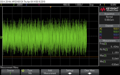 |
| To measure the amplitude of the sound I used the command from the oscilloscope | > Measure > Type |
|---|---|
| Min | - 535mV |
| Max | + 518mV |
| Peak to Peak | 1.05V |
OpAmp non-inverting#
| Schematic | Rules for the Resistor and the Voltage |
|---|---|
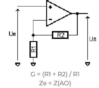 |
G = Gain, R2 could be a potentiometer, V depends on the gain. The output impendance is = to the OpAmp impedance |
| Learn Signal voltage | Comment |
|---|---|
 |
The goal for the Op Amp is to scaling the signal In from +2V;-2V to +5V;-5V depends on the Amp and the power voltage (Gain calculation). |
| Learn negative power supply | Comment |
|---|---|
 |
the different Op Amp need different voltage to pull up the signal voltage on the right position. For this part you could have a supply from +15V to - 15V |
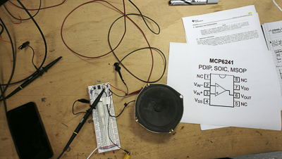
6 MCP6241#
| Providers | Datasheet |
|---|---|
| Op Amp MCP 6241 | DataSheet MCP6241 |
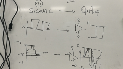
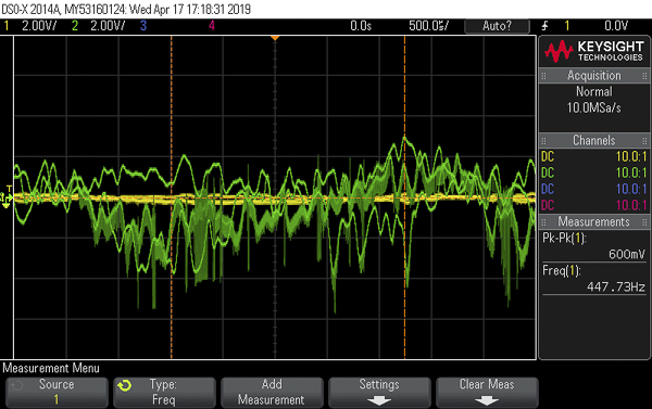
Using another opamp we had in stock in the electronics lab, I learned to compare input(yellow) and output(green) signals on an oscilloscope to understand the amplifacation factor (gain). From analyzing the signals I could tell that the problem with my circuit was that the signal was not centered on 0volts but was offset. This was cutting the signal in half (clipping).
| Protoboard | Oscilloscope |
|---|---|
 |
 |
Conclusion : The circuit is not good because we see that the amp doesn’t put the output signal in the center (at à Volts). I tried to solve this with a blocking capacitor but then became aware that there was an easier way which was to use a dedicated audio opamp, the LM386.
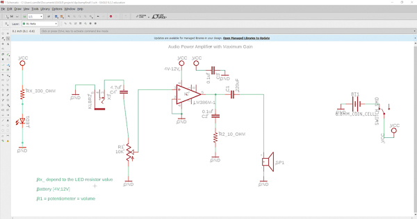
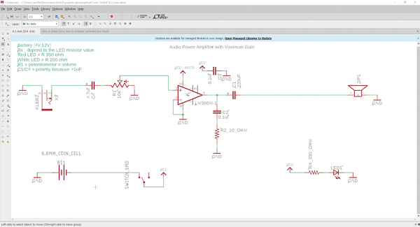
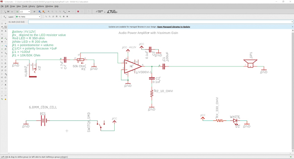
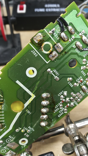
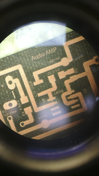
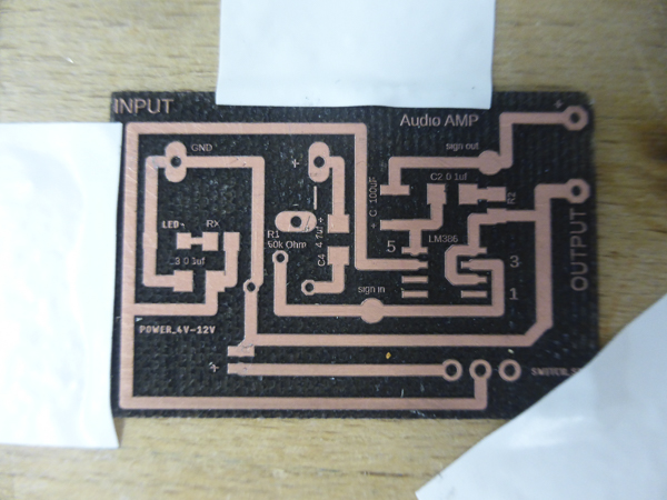
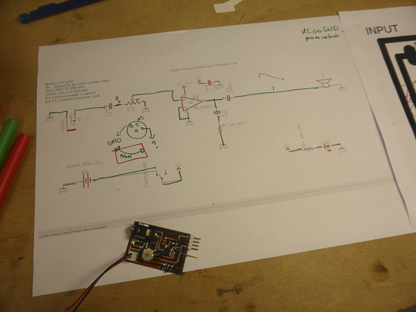
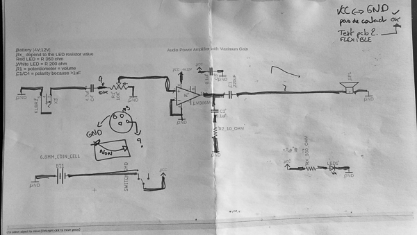
7 LM386#
| the Art (Bible) of Electronics | proposed LM386 circuit | LM386 circuit from TI datasheet |
|---|---|---|
 |
 |
 |
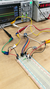
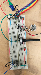
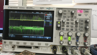
ProtoBoard Test#
| Protoboard | Protoboard detail | Oscilloscope Signal In and Signal Out Voltage |
|---|---|---|
 |
 |
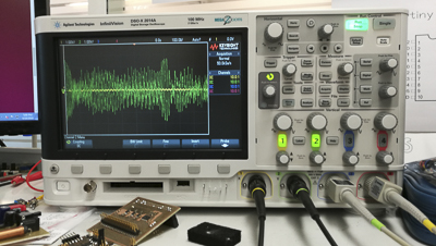 |
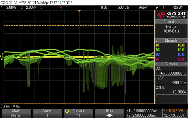
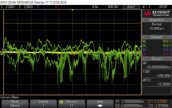
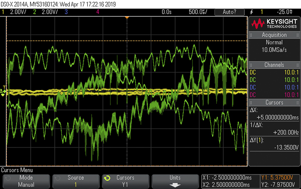
Using the skills I learned in previous experiments I was able to successfully build this circuit and confirm with the oscilloscope that everything was working as it should.
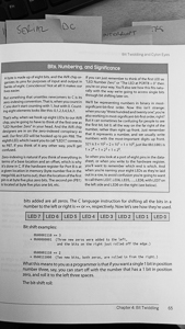
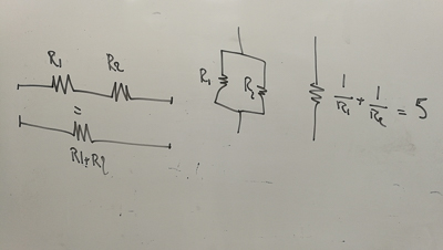
| Add a LED Serial/Parallel | Calculation of the resistor Value depends to the LED colors |
|---|---|
 |
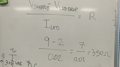 |
| Serial Rt = R1 + R2 / Parallel Rt = 1/R1 + 1/R2 | R for the Red with a 9V power supply LED is 350 Ohm |
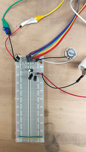
With this success I was able to add some new features to the ciruit. I wanted to add a switch for the user interface as well as an LED to give user feedback.
Depending on the parallel or series positioning of a resistor, the effective resistance value can be less than the value of the resitor. I learned how to calculate the reauired value of a resistor depending on the voltage supply and the specifications of the LED from the datasheet.
| Add a potentiometer 10k;50k and a red Led and an interrupter |
|---|
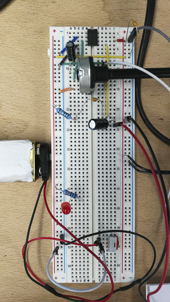 |
| Serial of tests with a cellphone and different flat spiral coil** |
|---|
 |
Video LM386#
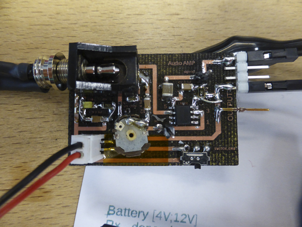
PCB Board Test#
To check the size and the block design part#
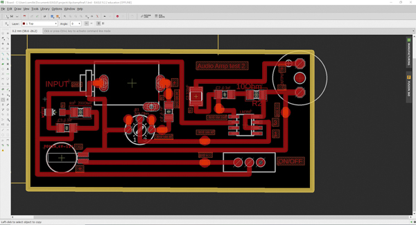
| Eagle | Eagle |
|---|---|
 |
 |
 |
 |
 |
 |
 |
 |
 |
 |
 |
 |
 |
 |
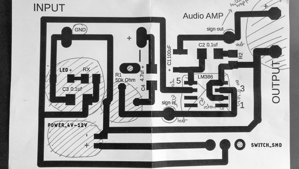
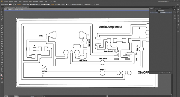
For this version of the amp, I designed thicker traces because I’m planning on making this circuit out of flexible fabric. I added text and symbols so that I could remember where the components should go and save time. I added test points to the circuit to make debugging easier. I found the output of Eagle visually interesting and felt that there was a graphic design research opportunity to explore this aesthetic further.
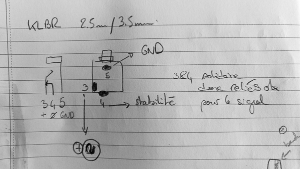
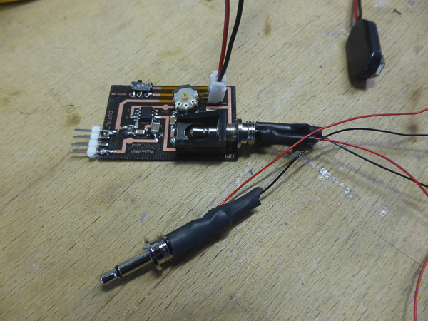
| The signal in (3.5mm audio-in jack) component | Desoldering the audio jack from a found radio | comment |
|---|---|---|
 |
 |
For the signal input, I recycled an old input device from a radio circuit. To desoler this part from the old board, I applied the soldering iron to the board and was able to reheat and remove the old solder, enabling me to remove the part. |
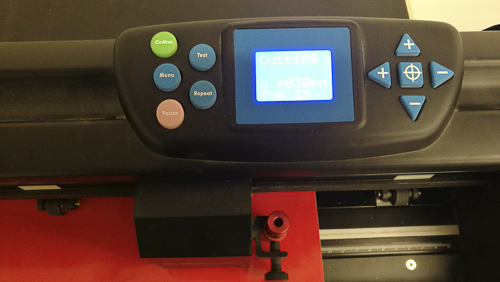
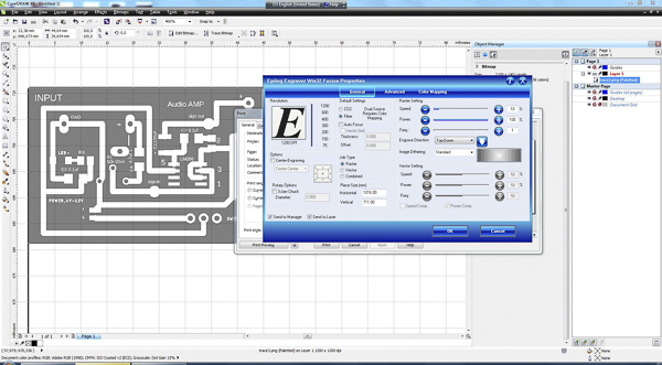
Lasercutting#
| To know how the signal travels trough the device I used the multimeter |
|---|
 |
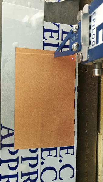
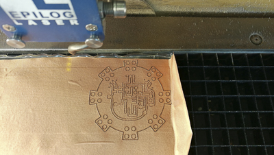
| Raster Epilog fusion | Cut Epilog Fusion |
|---|---|
 |
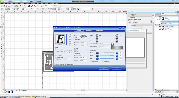 |
Previously I had tested different speeds and laser powers and I was able to draw on those past experiments to select the appropriate values for this engraving.
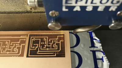
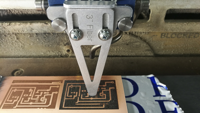
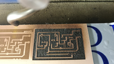
| Lasercut Raster Engraving | Fiber Z axis calibration after each pass | Final pass | Z lasercut CO2 for board cutting |
|---|---|---|---|
 |
 |
 |
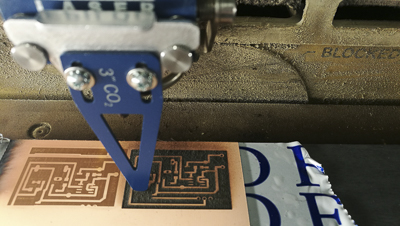 |
I changed the Z height after each pass to ensure the laser was perfectly focused for each pass.
| Clean with Alcool and silicone | Detail |
|---|---|
 |
 |
Under the microscope I could see if there were any tiny slivers which might cause shorts in my circuit.
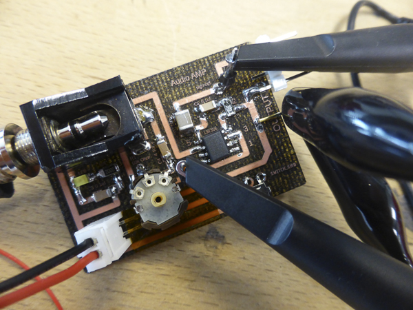
| Traces | Device |
|---|---|
 |
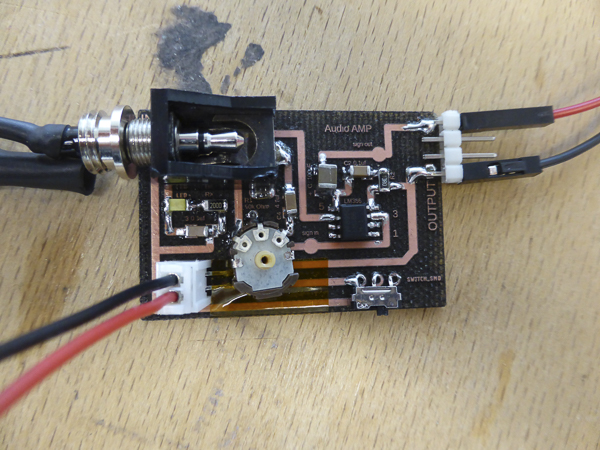 |
This time I protected the underside of the potentiometer with electrical tape and added heat shrink tubing to all of the connecting wires. I also chose specific connector typologies for different parts of the circuit.
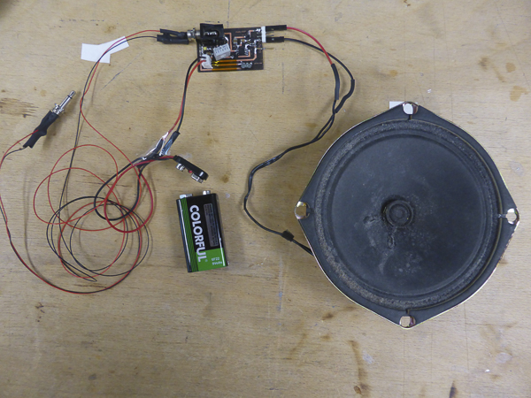
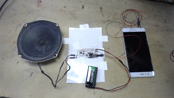
| Test | Cellphone and 8 Ohm speaker |
|---|---|
 |
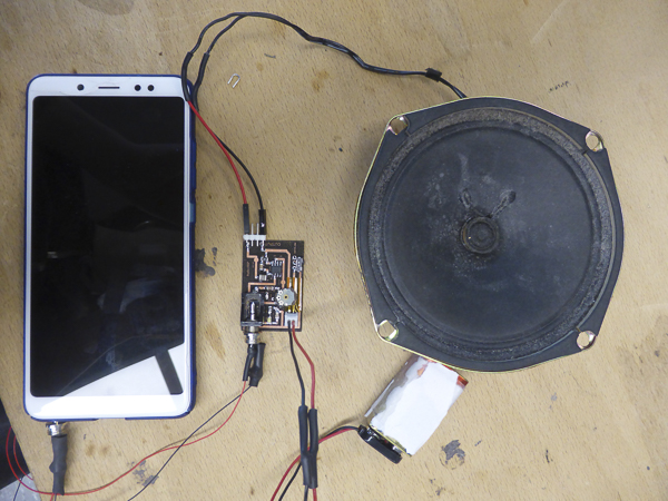 |
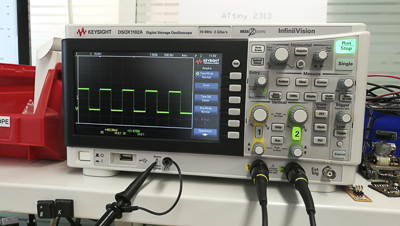
| Oscilloscope | Signal Out |
 |
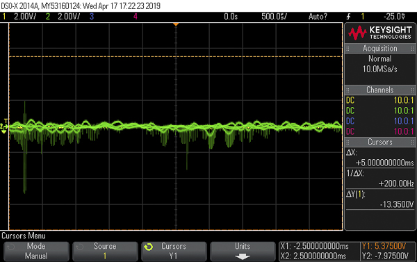 |
It works! I’m impressed with the amplication, it’s loud!
The signal is clear on the oscilloscope and is centered around zero volts.
| Test sheet circuit | problem solver | New test |
|---|---|---|
 |
 |
|
 |
My technique for debugging circuits involves printing the circuit schematic and then tracing over the connections I observe with a different color marker. I tested the continuity of each connection in the schematic on the board, each connecting wire, and ensured there was no short between positive and negative.
Work documents#
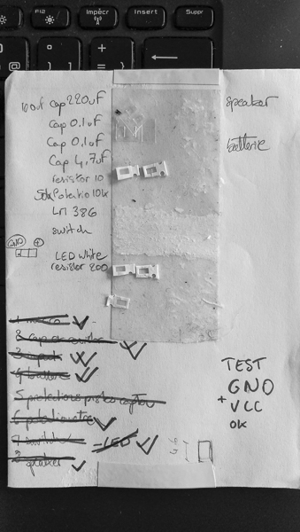
| Schematic tests | board test and reflexion | shopping list |
|---|---|---|
 |
 |
 |
Oscilloscope image#
Process
- One probe per signal and the aligator clip on ground.
- each square on the grid is 2V at this setting
- Navigating on the user interface to Meas > Type allows you to choose the Min and Max of the signal or measure the Peak to Peak voltage.
- Capture > Save > Save to save a screenshot to a usb key
| Oscilloscope beauty | Oscilloscope beauty |
|---|---|
 |
 |
 |
 |
Video oscilloscope signal#
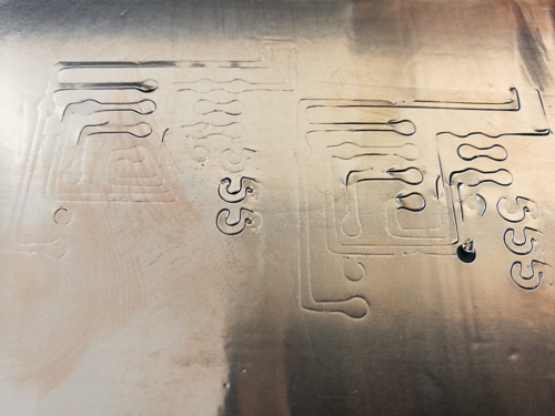
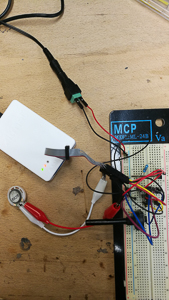
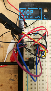
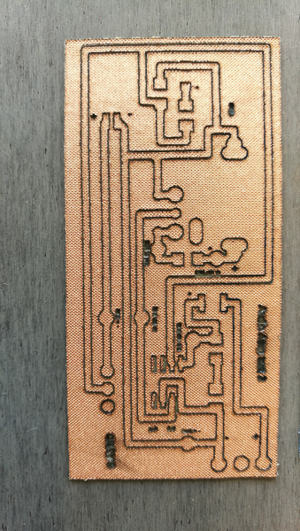
Copper Shield PCB test#
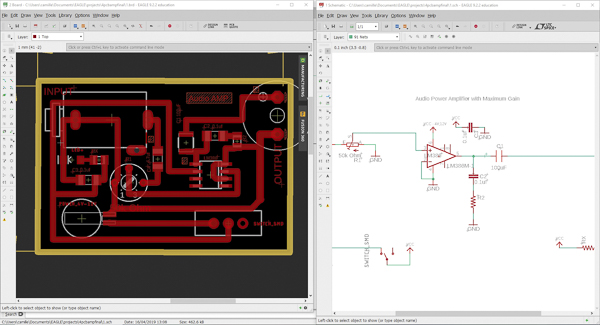
New file for a new optimisation of the circuit#
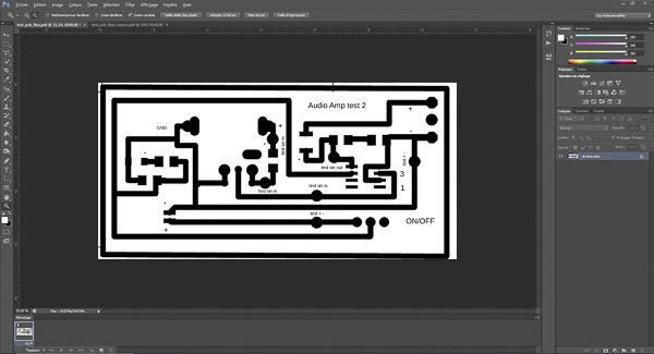
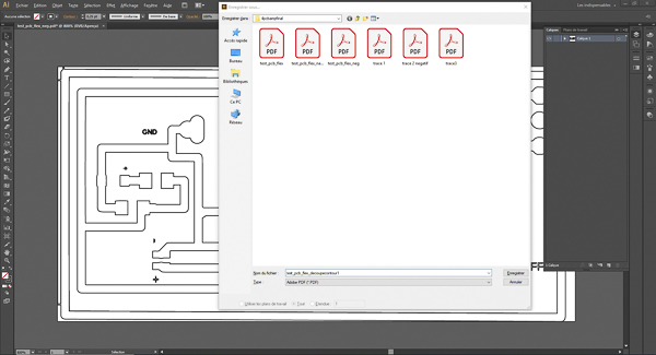
For the file I prefer to use Eagle and then Photoshop to change the trace for engraving or cutting and then illustrator for the vectorisation. The combination of these 3 software programs could be shorter but, I like to work with this protocol.
| Eagle | Photoshop |
|---|---|
 |
 |
| Illustrator Vectorisation | Illustrator save .pdf file |
 |
 |
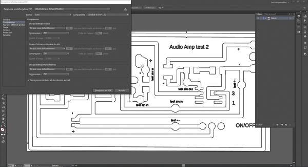 |
without compression |
Eagle exporting in PNG, then Photoshop importing an then exporting black and white to PDF? Illustrator Live Trace to identify the contours and exporting the final PDF.
Epoxy PBC versus Copper Fabric PCB#
| Laser cut the material Kapton + Copper shield | Result after lasercuted |
|---|---|
 |
 |
| Result on silk | Result on transparent sheet |
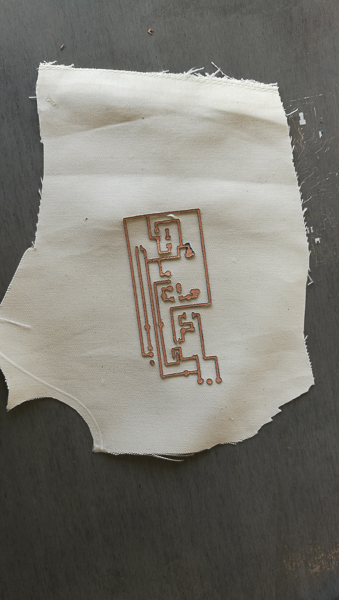 |
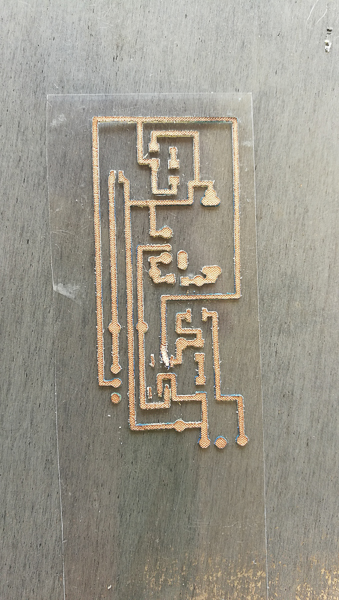 |
I was testing to see what the limits were for the thinnest possible circuit. I was searching for a new circuit materiality in a fabric form. I didn’t have the opportunity to explore this particular path more but I was able to test szitching the substrate pastic with bioplastic (shown in the following example).
| With the electronic part |
|---|
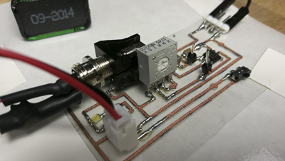 |
 |
This image shows the same electronic device but on a sheet a plastic instead of rigid epoxy. I followed the same debugging process.
I was dissapointed with the white connectors which I felt were inconsistent with the transparent aesthetic of the rest of the board.
| Test with cellphone and 8 Ohm Speaker |
|---|
 |
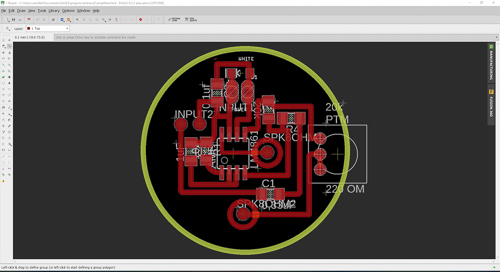
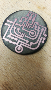
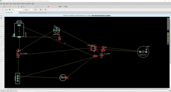
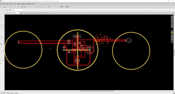
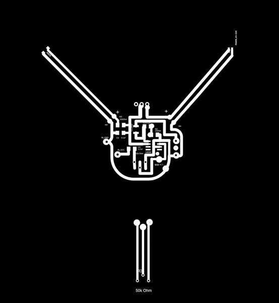
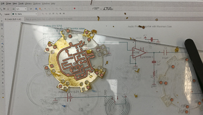
Circle PCB : 1206 size and modular parts#
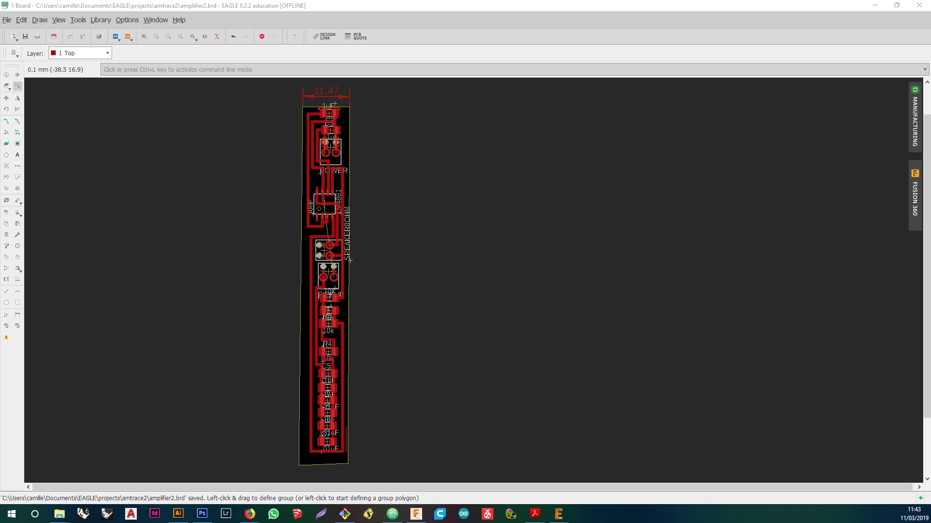
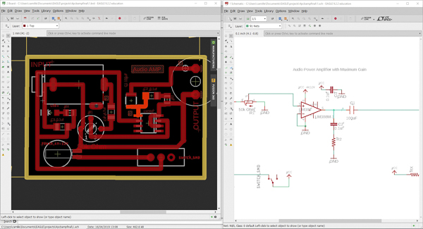
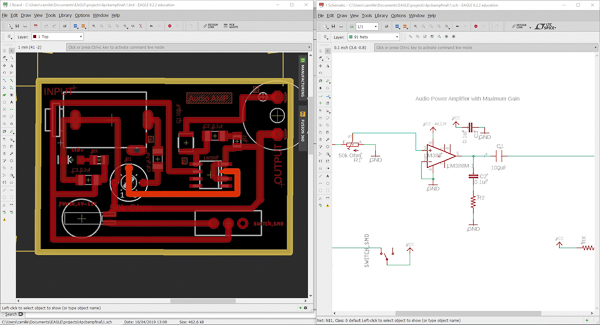
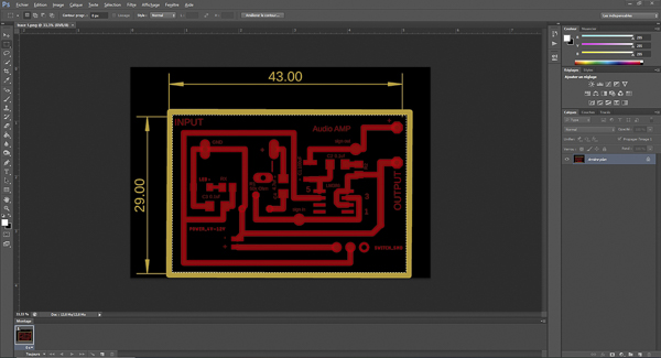
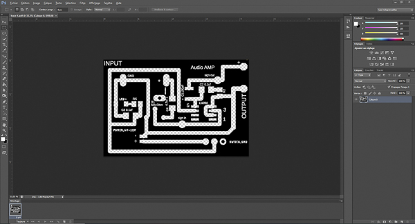
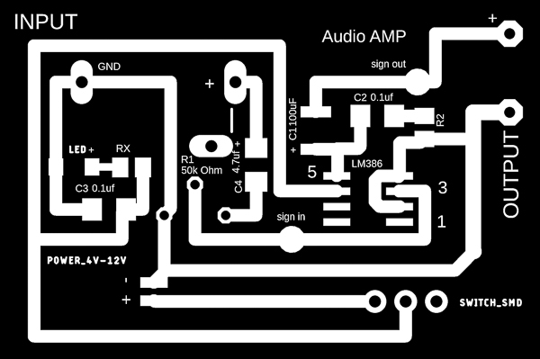
Now that I have a perfectly functioning circuit, I reworked my Eagle board design and tried to make a more compact design. I didn’t change the thickness of the traces in this version, I’m saving that for another experiment.
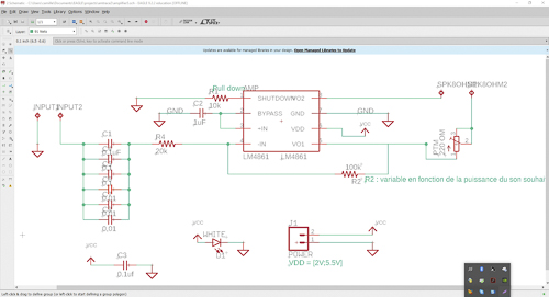
| Eagle Circuit Schematic Op Amp |
|---|
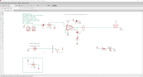 |
Nota Bene Detail : If you create a different + & - in add block, for example by adding both VCC and VDD or GND and gnd, you can create isolated circuits on the same board. In this schematic I have a completely isolated potentiometer on his own island.
| Eagle Circuit verification |
|---|
 |
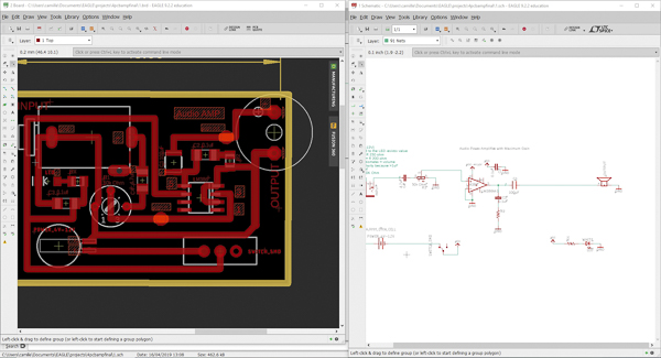
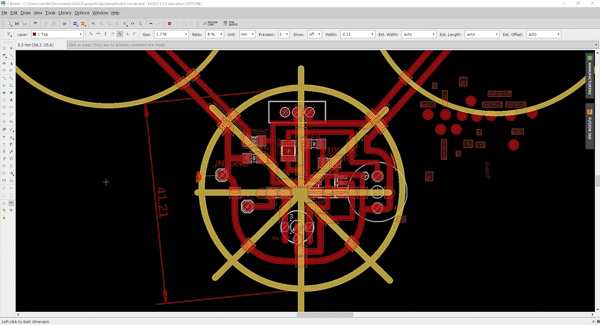
| Eagle design 1 | layer demension line | zoom |
|---|---|---|
 |
 |
 |
Here I am trying to explode the circuit, to explore its modular potential and to allow a user to be able to switch out different components and customize their circuit. (Please see following project pages for more description.)
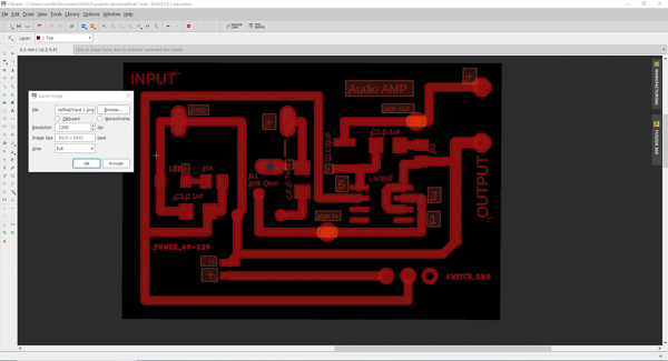
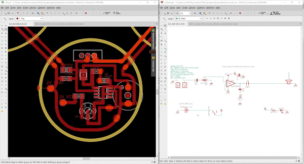
| Eagle Board LM 386 Op Amp | Trace |
|---|---|
 |
 |
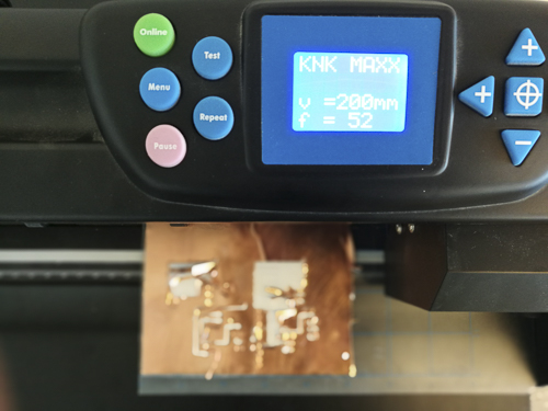
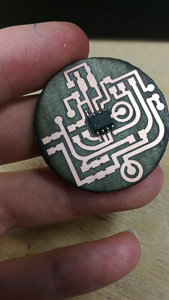
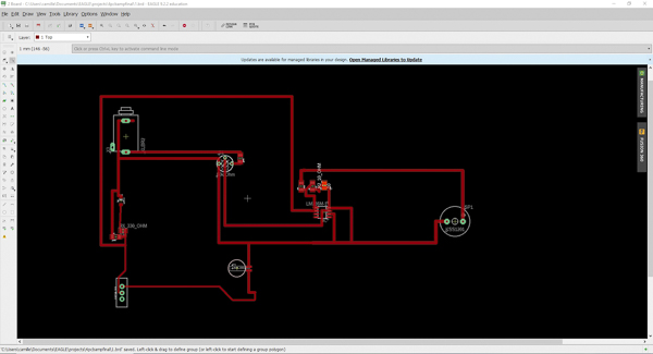
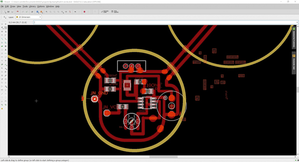
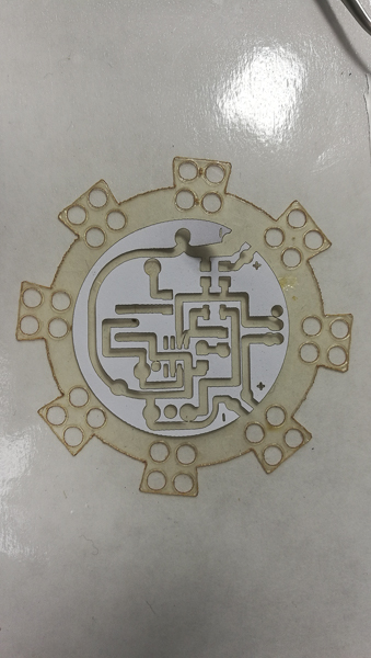
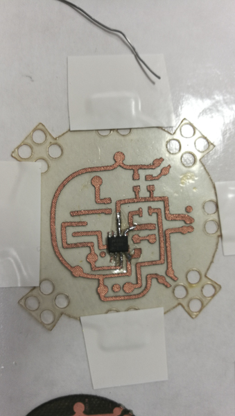
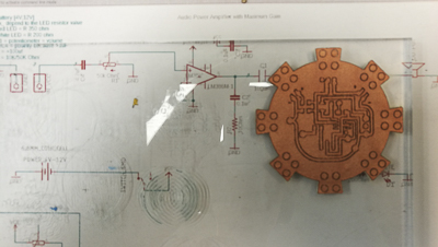
Circle PCB FR4 0,8mm#
| LM 386 Op Amp Raster Epilog with Fiber | Cut the contour with CO2 |
|---|---|
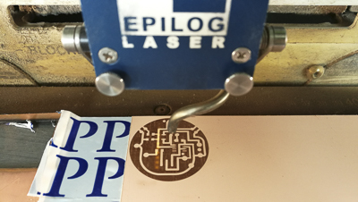 |
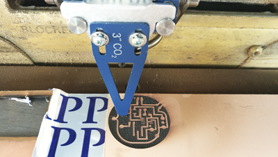 |
| Nota : you can check the Z axe with -20 at each pass | put the trace for the contour inside the black part if it doesn’t cut |
I have changed the board design and shape as well as some of the components. As a result, I have followed the debugging protocols I have developed to retest the functionality of the circuit.
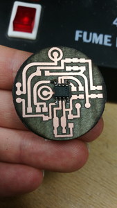
Video PCB FR4 lasercuted#
Video PCB FR4 LM 386 Op Amp device#
New circuit materiality#
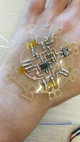
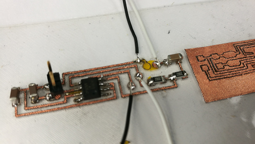
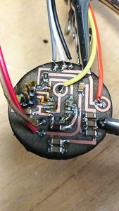
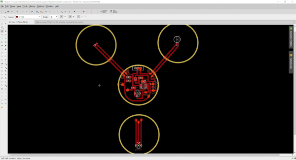
Circle PCB copper shield kapton on Bio-plastic material sheet#
In the introduction I tested two ways to affix the circuit on the plastic sheet:
- First cut the traces and then laminate it to the Kapton.
- Laminate first, then cut.
In the chapters that follow you’ll see why I chose the round form to make each module of my circuit. However, in this section I will focus on the making of the circuit itself.
| Putting the traces on | Soldering the op amp |
|---|---|
 |
 |
video bio-plastic home made sheet lasercuted#
video put the traces on the bioplastic shield#
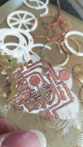
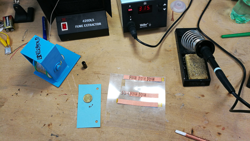
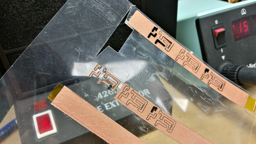
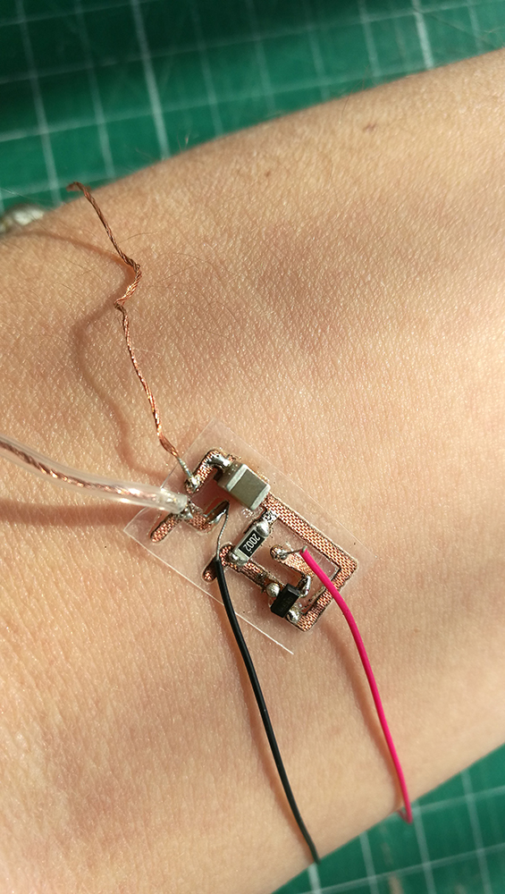
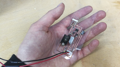
A very delicate process, similar to jewellery, which takes time to complete.
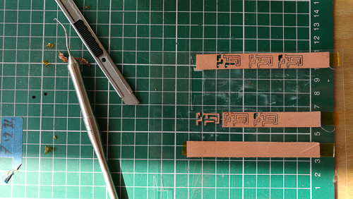
Circle PCB copper shield capton cut on Bio-platic material#
| laser cuted | result | without copper waste |
|---|---|---|
 |
 |
 |
This technique is more reliable because I only need to peel away the unwanted peices of copper frome the circuit.
video multilayered material : bio-plastic copper shield with capton lasercuted#
Video multilayered and bioplastic material#
| Parameters | Difficulties |
|---|---|
| Iron solder | In order to solder all the component I put the temperature at 250 °C. |
The technique of soldering on this laminate is very delicate and involved working with low temperature solering. With all of my practice over the course of the experients I have documented here, I was able to avoid cold solder joints and make reliable connections. Inspired by the art of Jewellery, I designed slender traces which invoked the elegant nature of this form of miniature construction. I feel at present that the circuit is far from perfect but I’ve found my own techniques to make circuits which question the standards of electronics manufacturing.