EEG circuit
Schematic
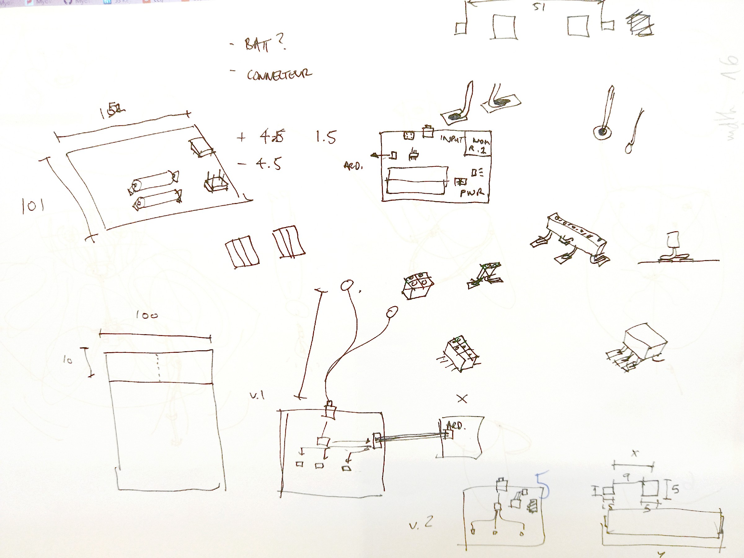
Just a brainstorm drawing
I found the documentation of the DIY EEG PCB of Elizabeth Ricker.
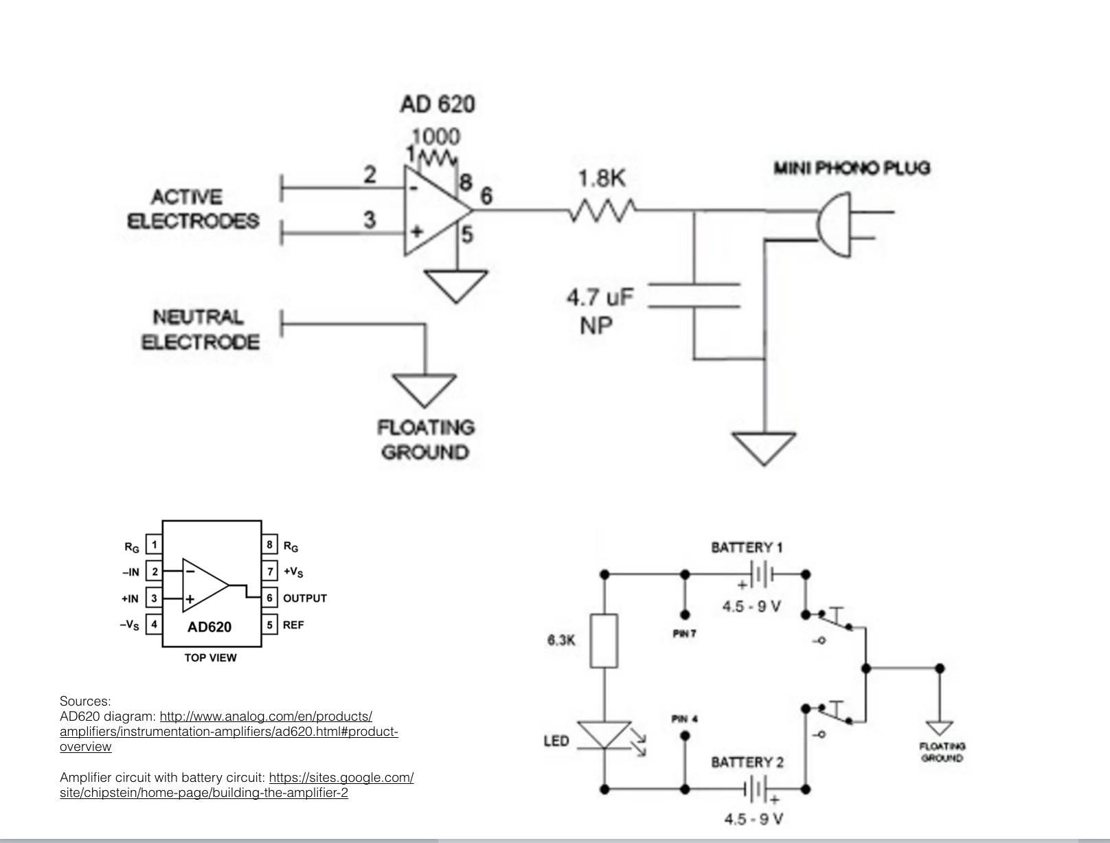
Elizabeth Ricker, EEG schematic.
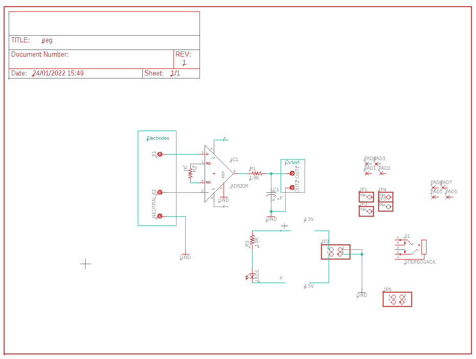
I took inspiration from her project and decided to change the EEG schematic to fit my project needs. To do so, I followed several tutorials on Eagle to learn how to do schematic and board. I adapted the EEG schematic to include a mini jack input (for the electrodes). Here is my Schematic (work in progress) :
Prototype
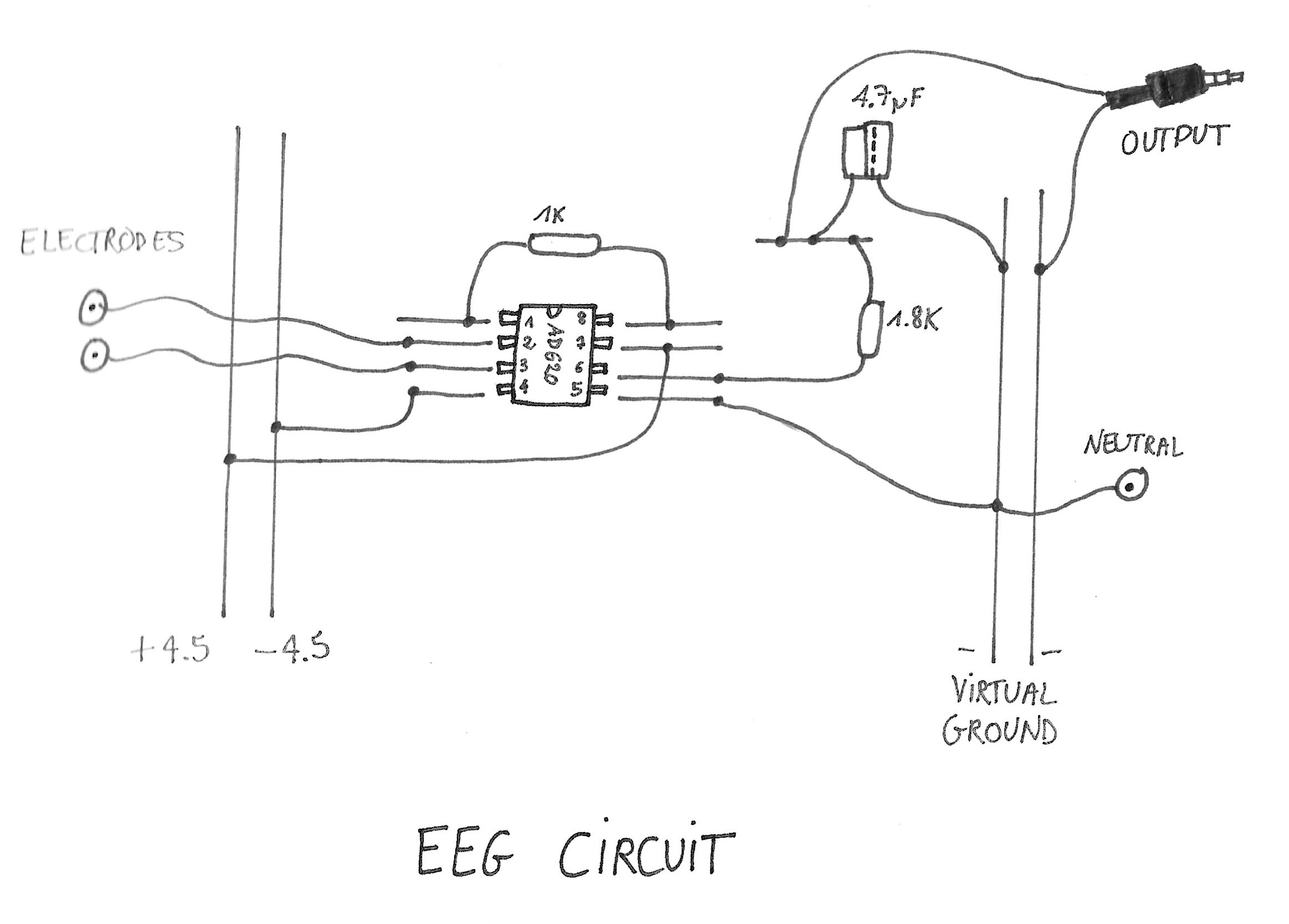
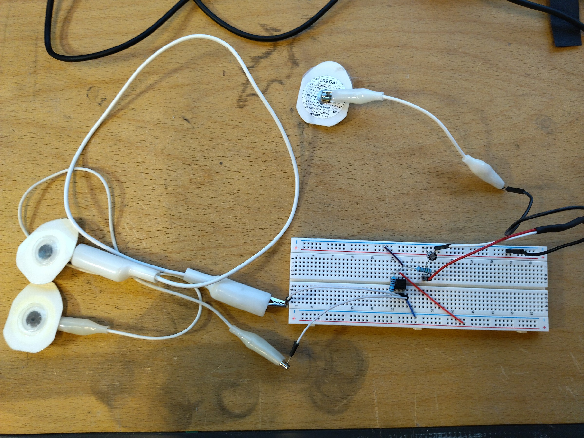
Since I got all the components for the EEG circuit, I made it first on breadboard. Here is a drawing of the circuit :
And the circuit on a breadboard :
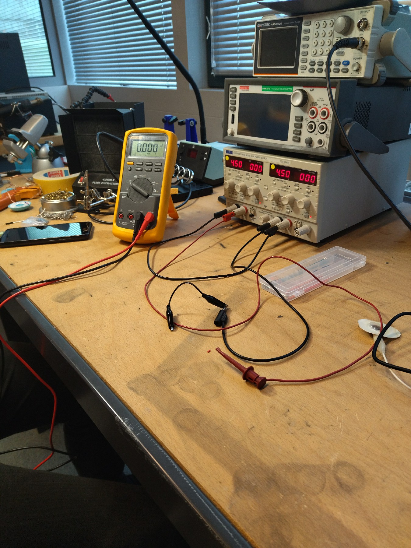
Testing the circuit
To test the circuit I used a multimeter, oscilloscope and function generator. I learnt how to use an oscilloscope and its different functions, especially :
- Zoom XY
- Calibrate the signal using square signal as a target : using a tiny screwdriver, turn the screw of the channel until the waveform is a square wave
Result of the manual signal calibration - Trigger a scope : to synchronize the voltage and time data of the signal, allowing to see a stable image of a repetitive waveform, so as to analyse it further and capture specific events.
- Measure
- Run
- Center the signal on the screen
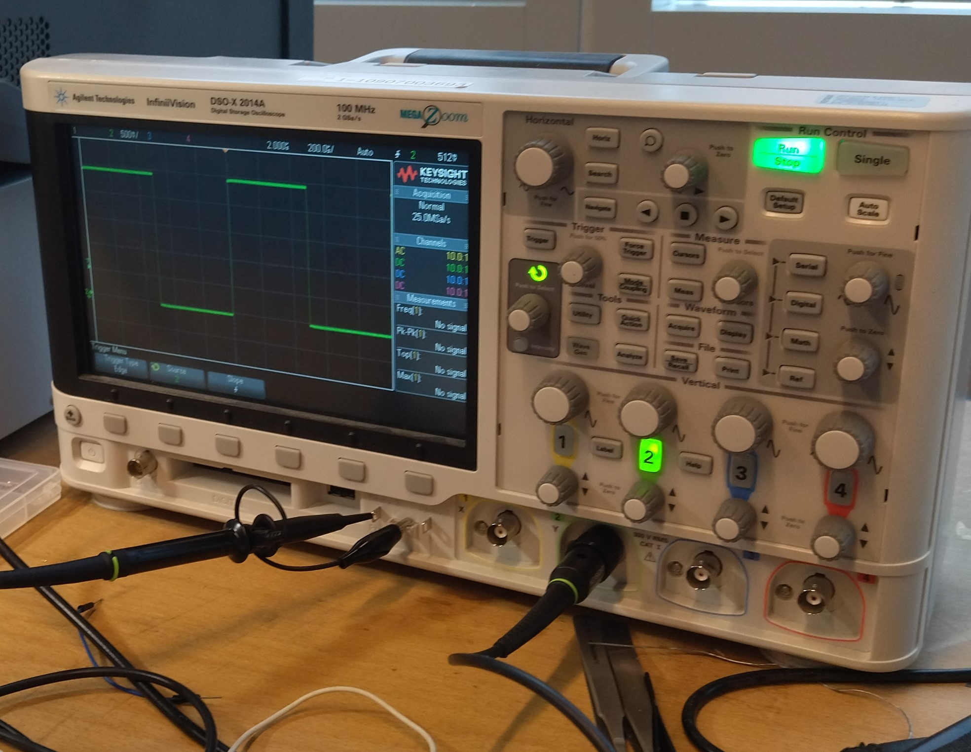
Common Mode Sense
Using the oscilloscope to measure the signal captured by the neutral electrode (Common Mode Sense), I found that the period was 20ms.
According to the formula of the frequency :
where T is the period.
In my case, Frequency = 1⁄20 = 50Hz. 50Hz is the average electrical interference in Europe, which is the value we expected.
Amplification
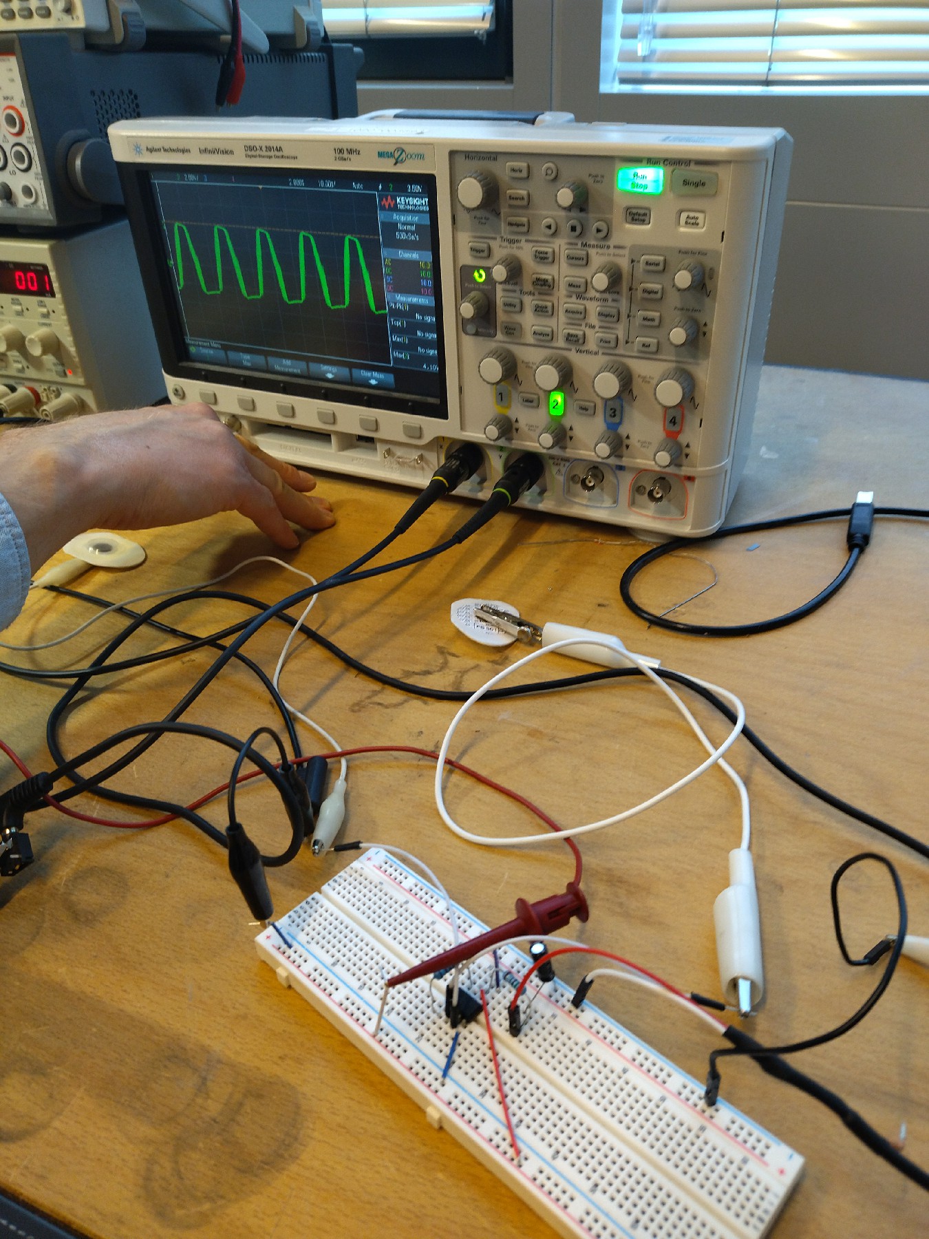
Before testing the circuit as a EMG or EEG, I wanted to ensure that the amplifier works correctly. To do so, I wired a function generator as an input of the amplifier, instead of the electrodes INPUT connected on pins 2 and 3 of the AD620.
Then, I connected the first channel (yellow) of the oscilloscope to the input of the circuit, and the second channel (green) to the ouput of the AD620 i.e. pin 6.
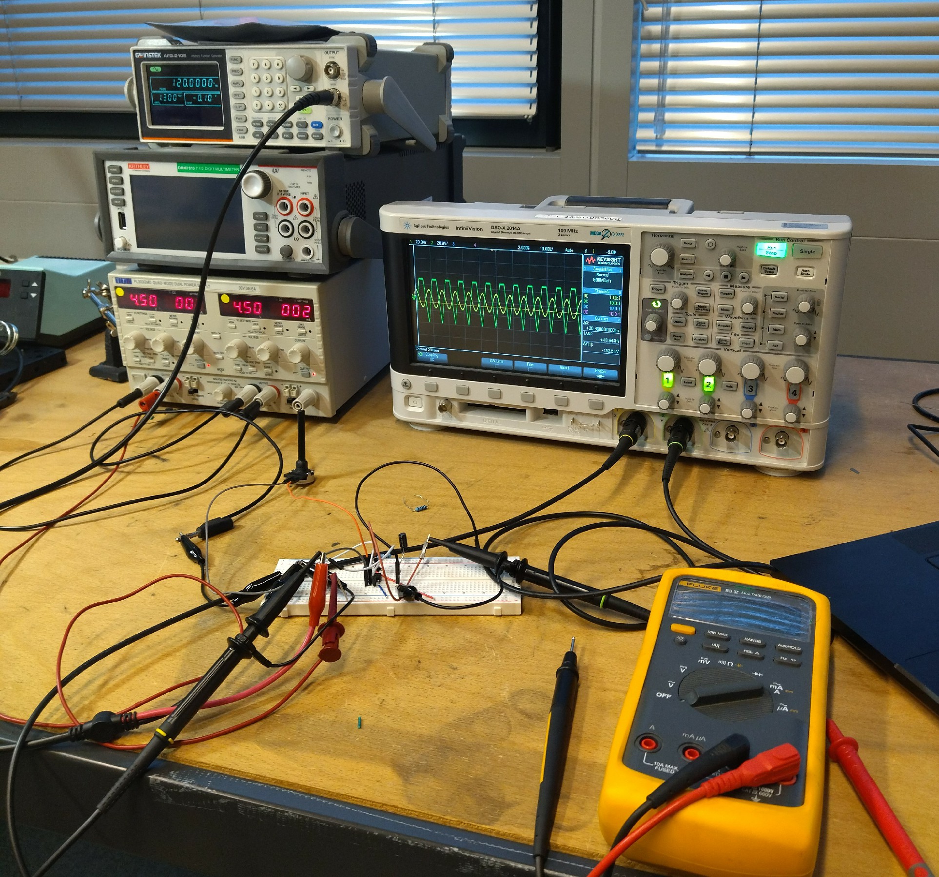
General wiring for the test
The amplification gain is proportional to the value of the resistor linking pins 1 and 8. The formula of the gain is :
where RG is the value of the resistor.
I replaced the 1K resistor of the circuit by a 10K potentiometer to test the amp with different value of gain.
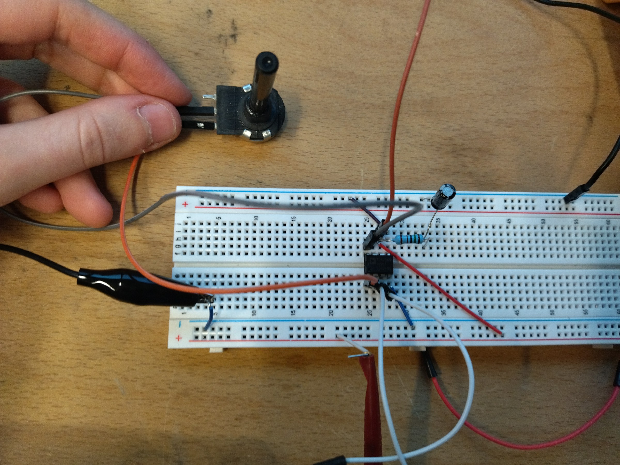
10K potentiometer replacing the resistor
.
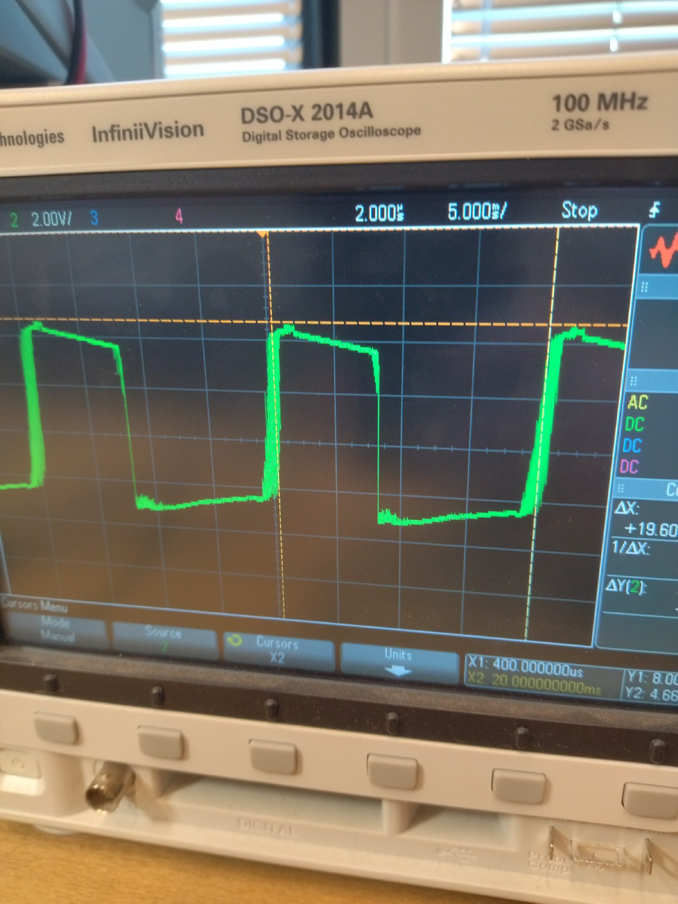
I noticed that no signal was amplified until I set specific values of the function generator. An example of values that worked for the AD620 is offset = - 0.10V, amplitude = 1.3 Vpp (peak-to-peak voltage) and frequency = 120kHz. The AD620 datasheet asserts that the amplififier has a bandwidth of 120 kHz (with Gain = 100). The range of correct values is something I should investigate.
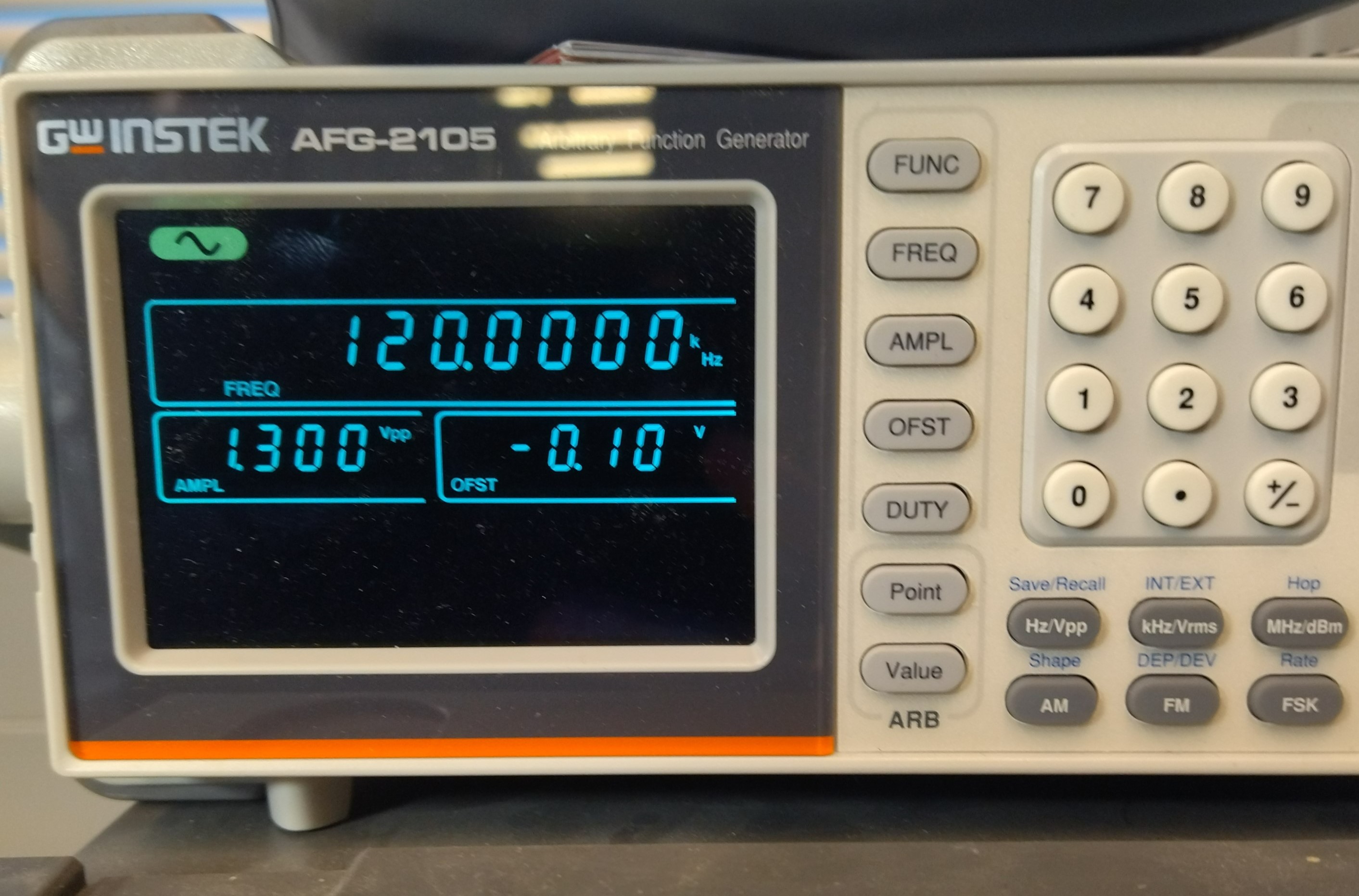
Function Generator with correct values
And the respective input and output signals displayed in the oscilloscope :
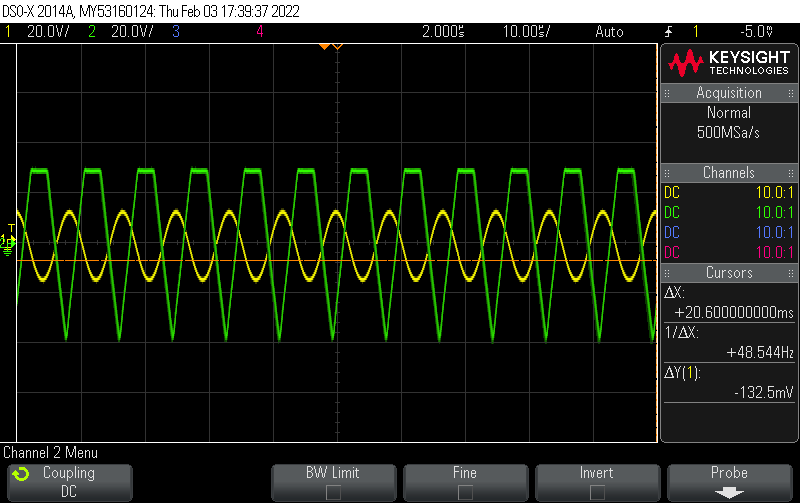
Signal given to the instrumentation amplifier (yellow), Signal amplified (green)
Electrodes
Once the amplifying circuit was working, I decided to test it with the electrodes. Since I don't want to use a digital power supply to power a circuit on my skin, I replaced it with LIPO batteries. Unfortunately I only had two 3.7V LIPO instead of 4.5V. First I placed the electrodes on my arm, because EMG and EEG circuit are the same (the only different is the gain value needed to amplify the signal).
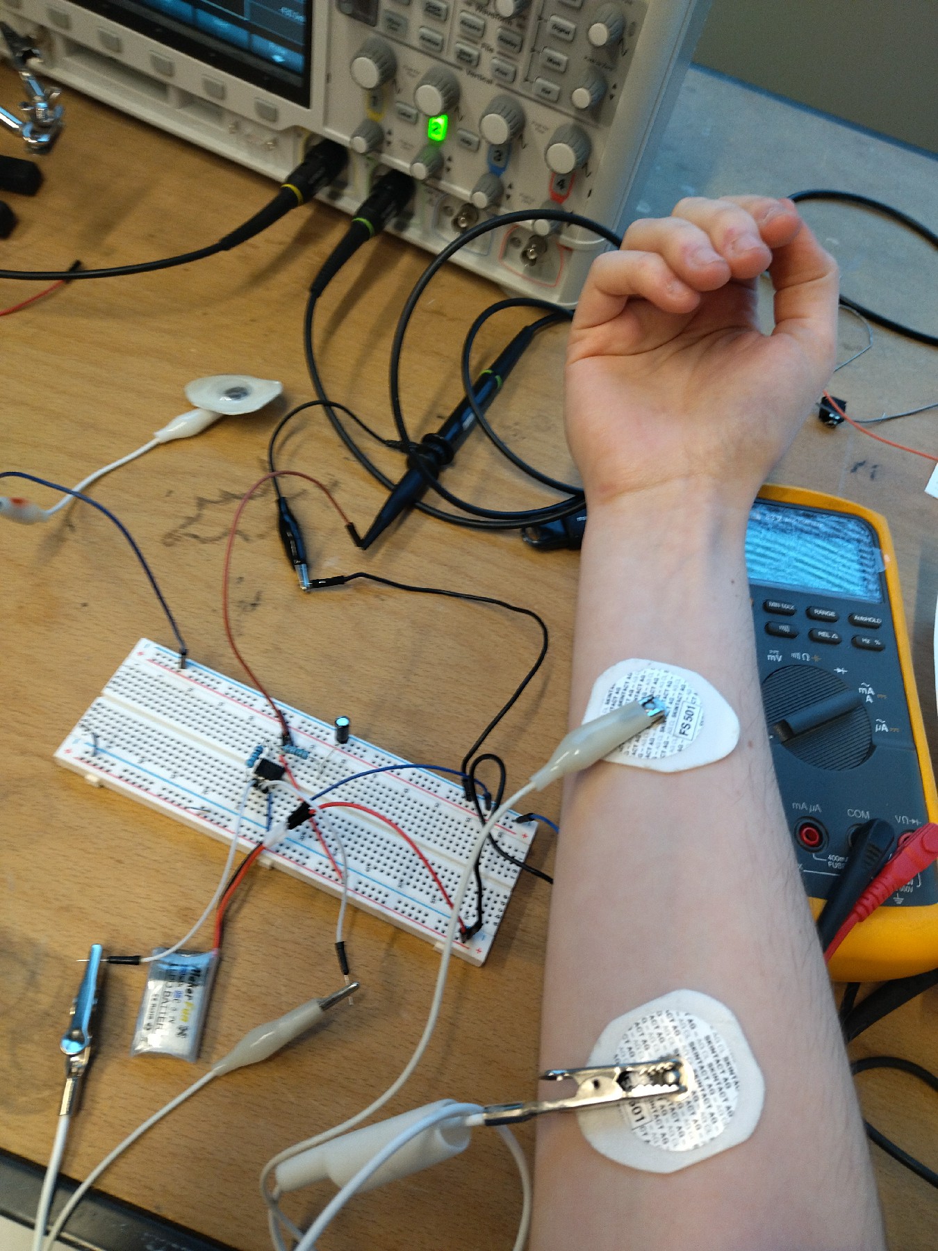
LIPO power supply for the EMG circuit
Afterwards, I tried the circuit as an EEG by placing the electrodes on my face at a specific placement : left prefrontal lobe (FP1), right prefrontal lobe (FP2) and left ear (A1).
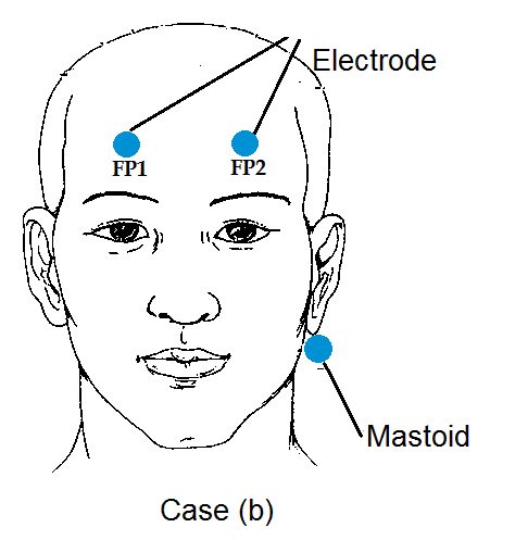
placement of electrodes used to observe a blink artifact in the signal, source : link
This placement of electrodes is supposed to help testing the EEG by displaying a blink artifact. At this point I am unsure whether the signal I observe in the oscilloscope is an EEG signal or it is just noise.
Electronics Theory
Virtual Ground
Op-Amp
Audio Output
I soldered jumpers to a raw mini jack cable (TODO : add photo)
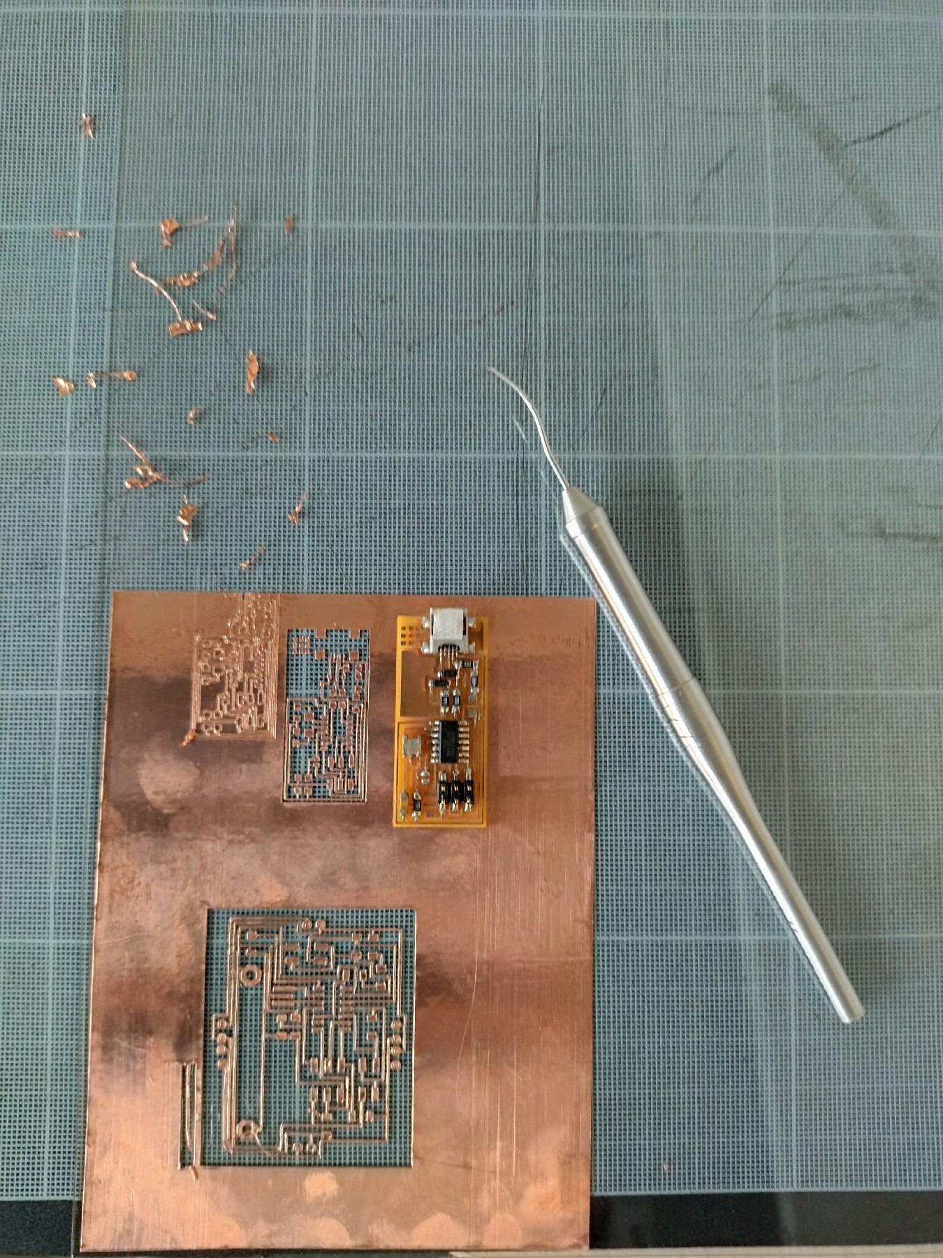
PCB Making
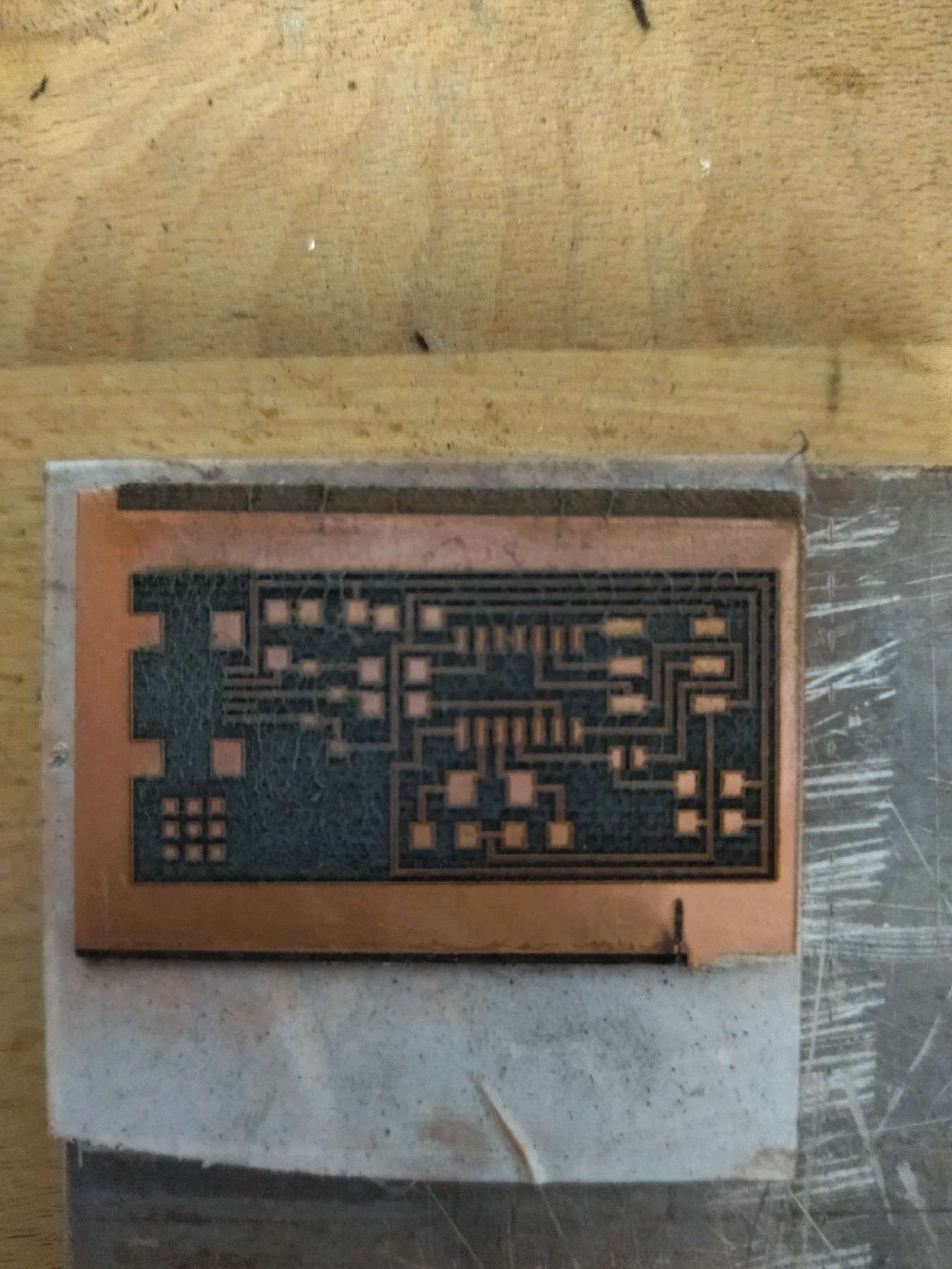
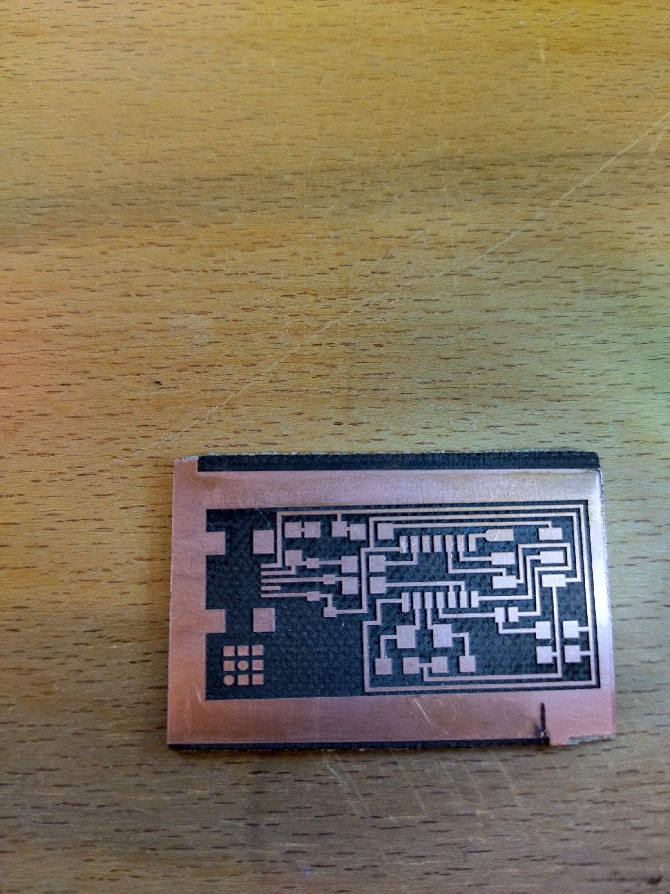
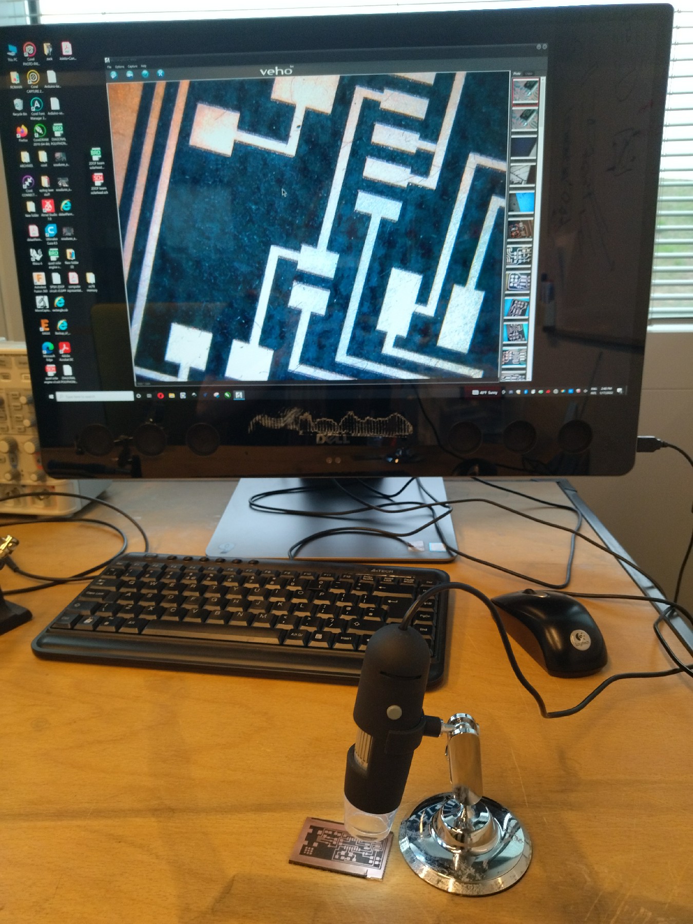
Fab ISP
To learn how to make a PCB, I was suggested by my local mentor to try to use different technics (laser cut and vinyl cutter) to make the PCB of an ISP programmer. I didn't conceive the PCB myself, the idea was only to learn how to make the physical board. Those traces comes from the CBA, see further documentation here.
Vinyl cutter
| 
|
Laser cut
| |
| 
|